Manufacturing of a semiconductor device with a reduced capacitance between wirings

a manufacturing method and technology of semiconductor devices, applied in semiconductor devices, semiconductor/solid-state device details, electrical apparatus, etc., can solve the problems of difficult control of shape after etching, damage to wirings, and significant increase in process number, so as to reduce the capacitance between wirings , the effect of uniform air gaps

Inactive Publication Date: 2006-09-26
NEC ELECTRONICS CORP
View PDF10 Cites 10 Cited by
  • Summary
  • Abstract
  • Description
  • Claims
  • Application Information

AI Technical Summary

Benefits of technology

[0013]Another object of the present invention is to provide a method of manufacturing a semiconductor device having a reduced capacitance between wirings in which the number of process step is reduced to simplify the process step. A further object of the present invention is to provide a method of stable manufacturing the semiconductor device.
[0034]In the step of forming a second trench, the insulating film may be removed using an etchant to selective removing the insulating film on the metal film without using a mask. As the insulating film, for instance, polyimide, especially photosensitive polyimide, may be utilized. As an etchant, hereat, hydrazine, for example, may be used. Thus, the insulating film alone is removed selectively without using a mask. As a result, in the step of forming a second trench, a second trench whose sidewalls are generally perpendicular to the bottom face can be formed and, thereby solving the problems in the conventional methods, uniform air gaps can be obtained.

Problems solved by technology

The use of a mask to form trenches to form air gap results in a significant increases in the number of processes.
Unlike this, the removal of the interlayer insulating film by dry etching without forming a mask may damage the wirings.
Moreover, as shown in FIGS. 1A and 1B, if an interlayer insulating film 1 is selectively removed by wet etching without forming a mask, shape after the etching becomes difficult to control.
As a result, even if via holes are formed in the wirings 5 and of low filling-up capability (i, e, the recesses are difficult to be filled up) to deposit an interlayer insulating film 6 therein, uniform air gaps 9 cannot be obtained.
This in turn deteriorates the adhesiveness between layers and increases the parasitic capacitance between wirings despite the use of the low-dielectric-constant material as the interlayer insulating film.

Method used


Image

  • Manufacturing of a semiconductor device with a reduced capacitance between wirings
  • Manufacturing of a semiconductor device with a reduced capacitance between wirings
  • Manufacturing of a semiconductor device with a reduced capacitance between wirings

Examples


first embodiment

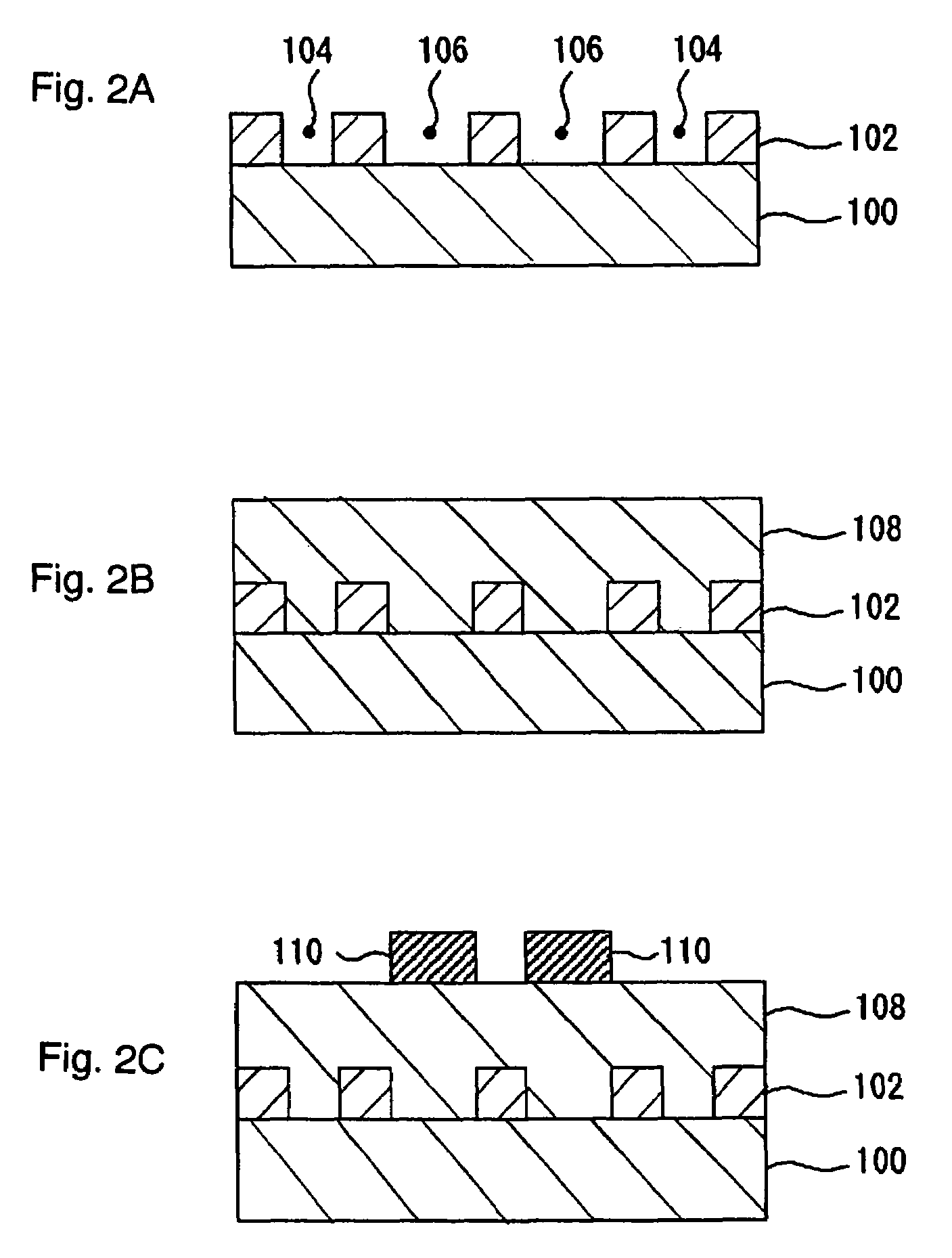
[0041]FIGS. 2A to 4B are schematic cross-sectional views illustrating the steps of a method of manufacturing a semiconductor device according to the first embodiment of the present invention. The steps of forming a multi-layered wiring structure by the dual damascene method are described below.

[0042]Firstly, on a semiconductor substrate 100, a first insulating film 102 (for example, with a thickness of 800 nm) is formed. The first insulating film 102, for example, may be made of a silicon oxide film. It is also possible for the first insulating film 102 to be composed of what is called a low-dielectric-constant material.

[0043]As a low-dielectric-constant material, various materials may be utilized and it is preferable to contain a ladder oxide such as a ladder hydrogenated siloxane therein. The ladder hydrogenated siloxane is a polymer with the ladder molecular structure, and preferably has a dielectric constant of 2.9 or less from the viewpoint of the wiring delay suppression. Pref...

second embodiment

[0057]FIGS. 5A to 5C are schematic cross-sectional views illustrating a part of the steps of a method of manufacturing a semiconductor device according to the second embodiment of the present invention.

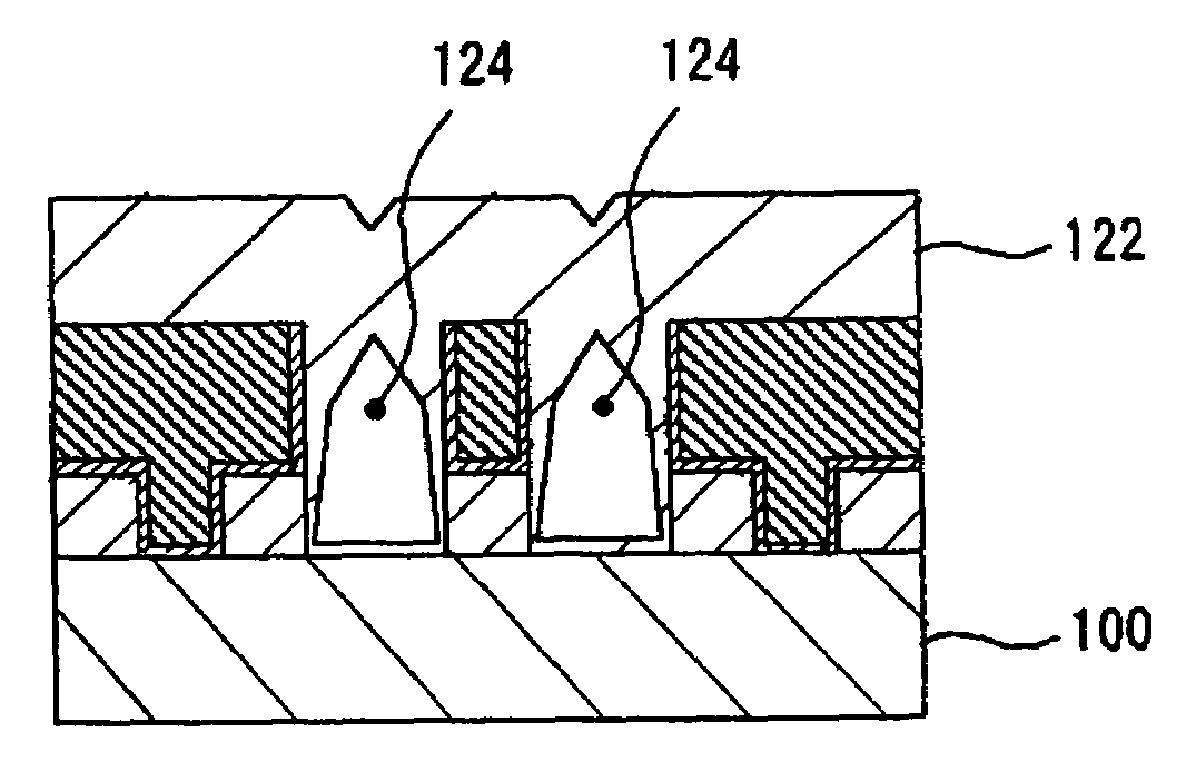
[0058]In the present embodiment, too, wirings 118, via plugs 119, and sacrifice films 112 are formed by the same method as described in the first embodiment with reference to FIGS. 2A to 3E. After that, as in the first embodiment, the sacrifice films 112 are selectively removed, for example, by selective wet etching with hydrazine, whereby, extending over the layer where the via plugs 119 are formed and the layer having the wirings 118 formed thereon, second trenches (same as the second trenches to form air gaps in the first embodiment) 120 whose sidewalls are generally perpendicular to the bottom face of the first trenches (same as the first trenches to form air gaps in the first embodiment) 106 (see FIGS. 2A to 2C) are formed (see FIG. 5A).

[0059]In the present embodiment, a third in...


PUM


Abstract

In the method of manufacturing a semiconductor device, via holes and first trenches to form air gaps are concurrently formed in a first insulating film on a semiconductor substrate and a second insulating film is formed thereon. Thereafter, the second insulating film lying outside the area corresponding to the regions where the first trenches to form air gaps are formed is partially removed to form trenches for wiring by using a mask. A plurality of wirings are formed by filling in the trenches for wiring with a metal film. The second insulating film remaining in the regions where the first trenches to form air gaps are formed is then removed to form second trenches to form air gaps. Subsequently, in forming a third insulating film, air gaps are formed within the second trenches to form air gap.

Description

BACKGROUND OF THE INVENTION[0001]1. Field of the Invention[0002]The present invention relates to a method of manufacturing a semiconductor device.[0003]2. Description of the Related Art[0004]To reduce parasitic capacitance between wiring when fabricating semiconductor devices with multi-layered wiring structures on a semiconductor substrate, a low-dielectric-constant material has heretofore been used as the interlayer insulating film or air gaps (cavities) are formed between wiring.[0005]The latter is disclosed, for example, in Japanese Patent Application Laid-open No. 85519 / 2001. In this publication, wirings having a reversed taper configuration on a sacrifice layer are formed made up of, for example, PSG (Phosphorous Silicate Glass) and the sacrifice layer is removed by dry etching or wet etching to thereby form air gaps between wirings.[0006]Japanese Patent No. 3102382 discloses a semiconductor device and a method of manufacturing the same in which openings of via holes and openi...

Claims


Application Information

Patent Timeline
Patent Type & Authority Patents(United States)
IPC IPC(8): H01L21/4763H01L21/44H01L23/522H01L21/768
CPCH01L21/76807H01L21/7682H01L21/76837H01L21/76835H01L2221/1031
Inventor OKADA, MAKOTO
Owner NEC ELECTRONICS CORP
Why Eureka
Try Eureka