Electronic device
a technology of electronic devices and corresponding devices, applied in the field of electronic displays, can solve problems such as inability to achieve desired gray-scale (tone) and unsatisfactory situations
- Summary
- Abstract
- Description
- Claims
- Application Information
AI Technical Summary
Benefits of technology
Problems solved by technology
Method used
Image

Examples
embodiment 1
[0245]In the EL display of the present invention, a case of performing a 26 gray-scale display from a 6-bit digital data signal is explained in Embodiment 1 with reference to FIG. 5. It is to be noted that the EL display of Embodiment 1 has the structure that is illustrated in FIGS. 1 to 3.
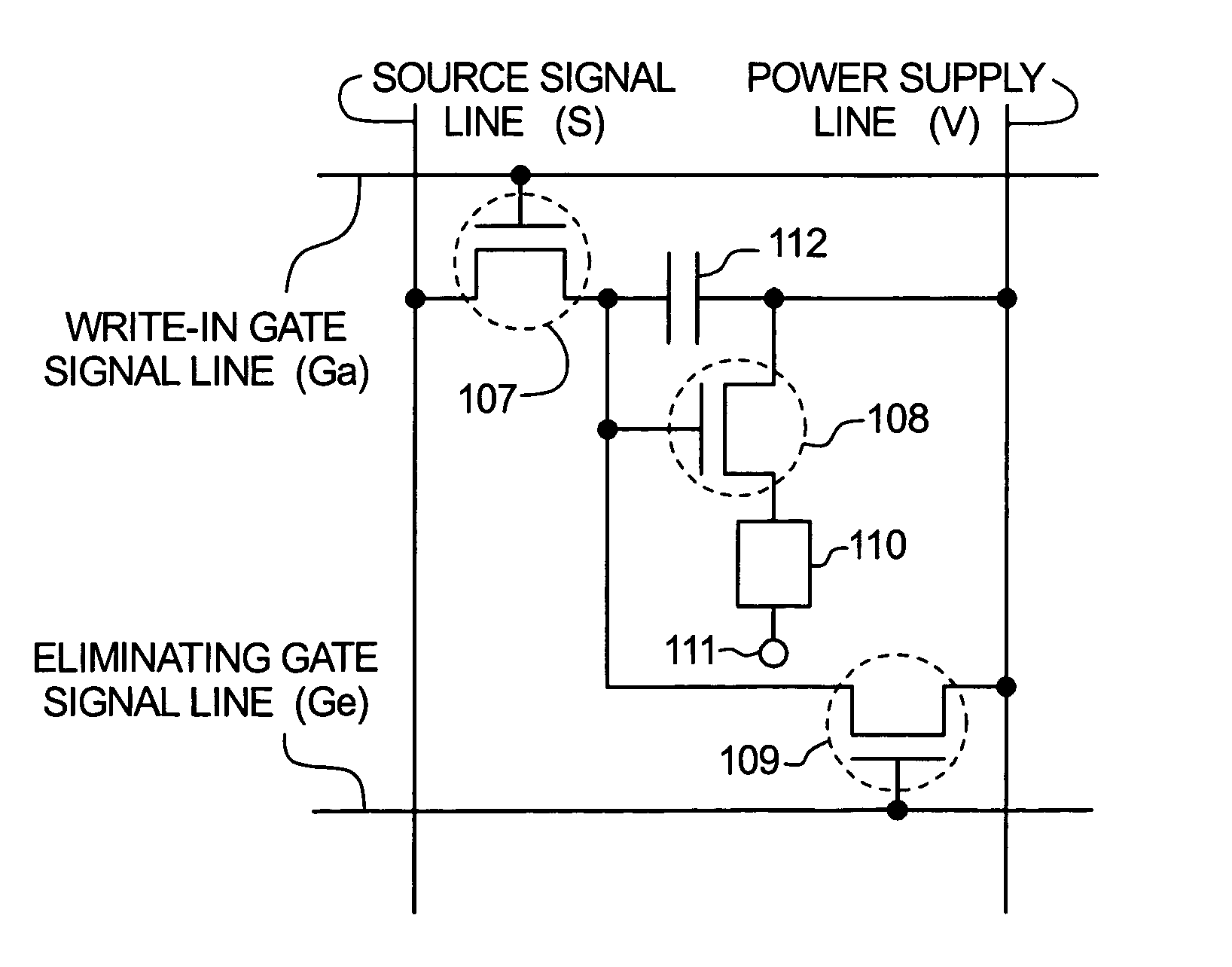
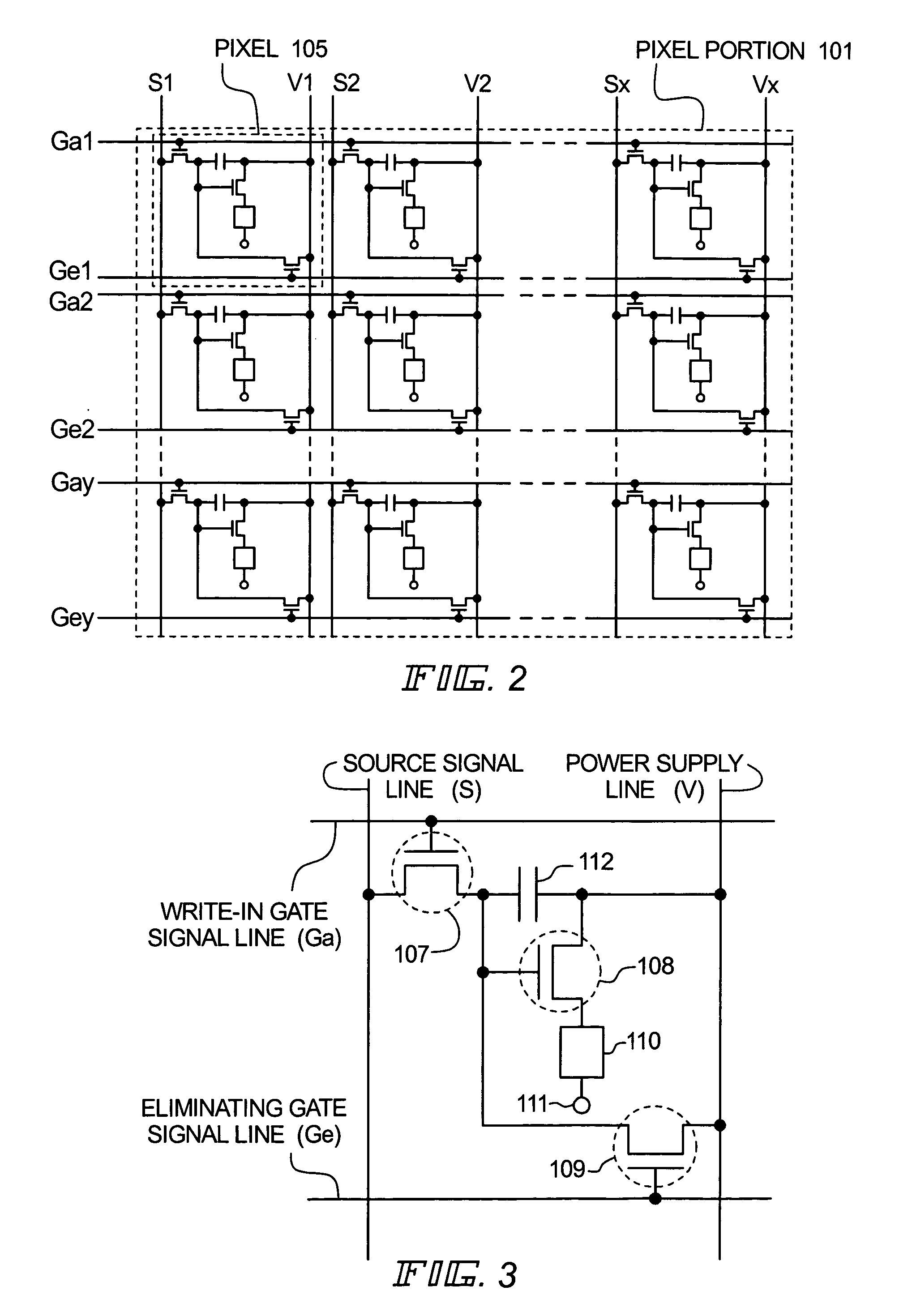
[0246]First, the writing-in selecting signal from the writing-in gate signal line driver circuit 103 is fed to the writing-in gate signal line Ga1. As a result, the switching TFTs 107 of all the pixels (pixels of the first line) connected to the writing-in gate signal line Ga1 are turned to the ON state.
[0247]And at the same time, the first bit of the digital data signal from the latch circuit (B) 102c of the source signal line driver circuit 102 is fed to the source signal lines S1 to Sx. The digital data signal is fed to the gate electrode of the EL driving TFT 108 through the switching TFT 107.
[0248]In the Embodiment 1, when the digital data signal has the “0” information, the EL driving TFT 10...
embodiment 2
[0277]An example of manufacturing an EL display using the present invention is explained in embodiment 2.
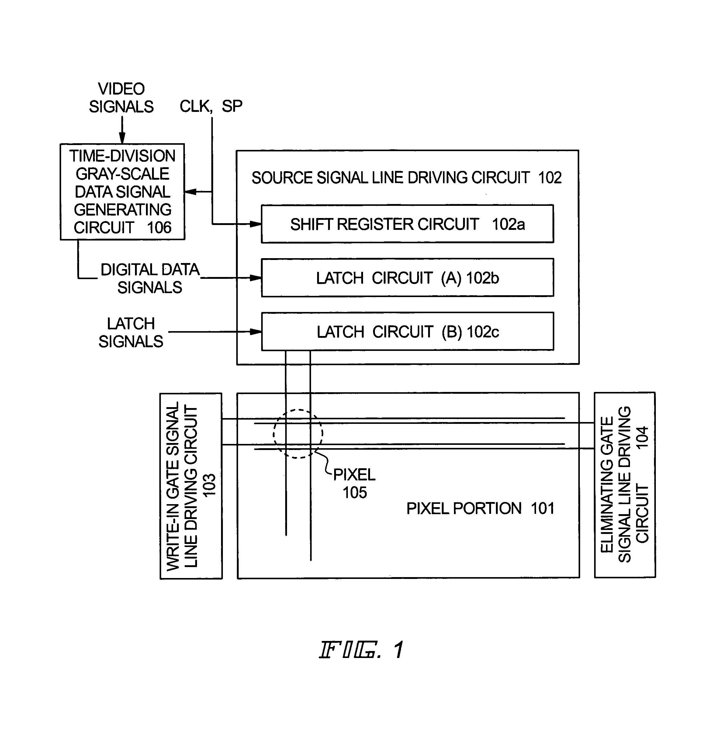
[0278]FIG. 6A is a top view of an EL display device using the present invention. In FIG. 6A, reference numeral 4010 is a substrate, reference numeral 4011 is a pixel portion, reference numeral 4012 is a source signal line driver circuit, reference numeral 4013a is a writing gate signal line driver circuit and 4013b is an erasing gate signal line driver circuit. The driver circuits are connected to external equipment, through an FPC 4017, via wirings 4014a, 4014b, 4015 and 4016.
[0279]A covering material 6000, a sealing material (also referred to as a housing material) 7000, and an airtight sealing material (a second sealing material) 7001 are formed so as to enclose at least the pixel portion, preferably the driver circuits and the pixel portion, at this point.
[0280]Further, FIG. 6B is a cross sectional structure of the EL display device of the present invention. A driver circuit ...
embodiment 3
[0296]In this embodiment, an example of manufacturing an EL display device having a structure which differs from that of embodiment 2 is explained using FIGS. 7A and 7B. Parts having the same reference numerals as those of FIGS. 6A and 6B indicate the same portions, and therefore an explanation of those parts is omitted.
[0297]FIG. 7A is a top view of an EL display device of this embodiment, and FIG. 7B shows a cross sectional diagram in which FIG. 7A is cut along the line A–A′.
[0298]In accordance with embodiment 2, manufacturing is performed through the step of forming the passivation film 6003 covering the EL element.
[0299]In addition, the filling material 6004 is formed so as to cover the EL element. The filling material 6004 also functions as an adhesive for bonding the covering material 6000. PVC (polyvinyl chloride), epoxy resin, silicone resin, PVB (polyvinyl butyral), and EVA (ethylene vinyl acetate) can be used as the filling material 6004. If a drying agent is provided on t...
PUM
 Abstract
Description
Claims
Application Information
 - Generate Ideas
- Intellectual Property
- Life Sciences
- Materials
- Tech Scout
- Unparalleled Data Quality
- Higher Quality Content
- 60% Fewer Hallucinations
Browse by: Latest US Patents, China's latest patents, Technical Efficacy Thesaurus, Application Domain, Technology Topic, Popular Technical Reports.
© 2025 PatSnap. All rights reserved.Legal|Privacy policy|Modern Slavery Act Transparency Statement|Sitemap|About US| Contact US: help@patsnap.com