Clock recovery circuit and receiver circuit for improving the error rate of signal reproduction

a clock recovery circuit and error rate technology, applied in the direction of digital transmission, amplitude demodulation, instruments, etc., can solve the problems of slow signal transmission speed between a main storage device such as a dram and a processor, affecting the performance improvement of the computer as a whole, and the inability to improve system performance further, so as to achieve enhanced accuracy and reduce the jitter dependence and signal level dependence of feedback loop characteristics.

Inactive Publication Date: 2006-10-03
FUJITSU LTD
View PDF10 Cites 48 Cited by
  • Summary
  • Abstract
  • Description
  • Claims
  • Application Information

AI Technical Summary

Benefits of technology

[0010]An object of the present invention is to provide a clock recovery circuit and a receiver circuit wherein limit cycle signal amplitude is small and the jitter dependence and signal level dependence of feedback loop chara

Problems solved by technology

The improvements in the performance of semiconductor memory devices, processors, and the like have reached the point where system performance cannot be improved further unless the speed of signal transmission between components or elements is increased.
Specifically, the speed of signal transmission between a main storage device such as a DRAM and a proc

Method used


Image

  • Clock recovery circuit and receiver circuit for improving the error rate of signal reproduction
  • Clock recovery circuit and receiver circuit for improving the error rate of signal reproduction
  • Clock recovery circuit and receiver circuit for improving the error rate of signal reproduction

Examples


first embodiment

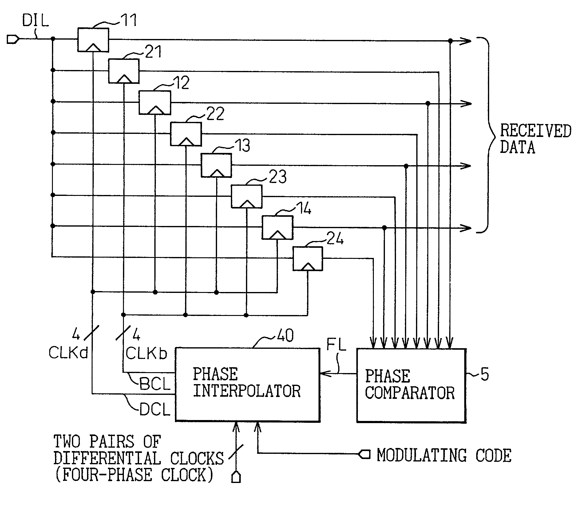
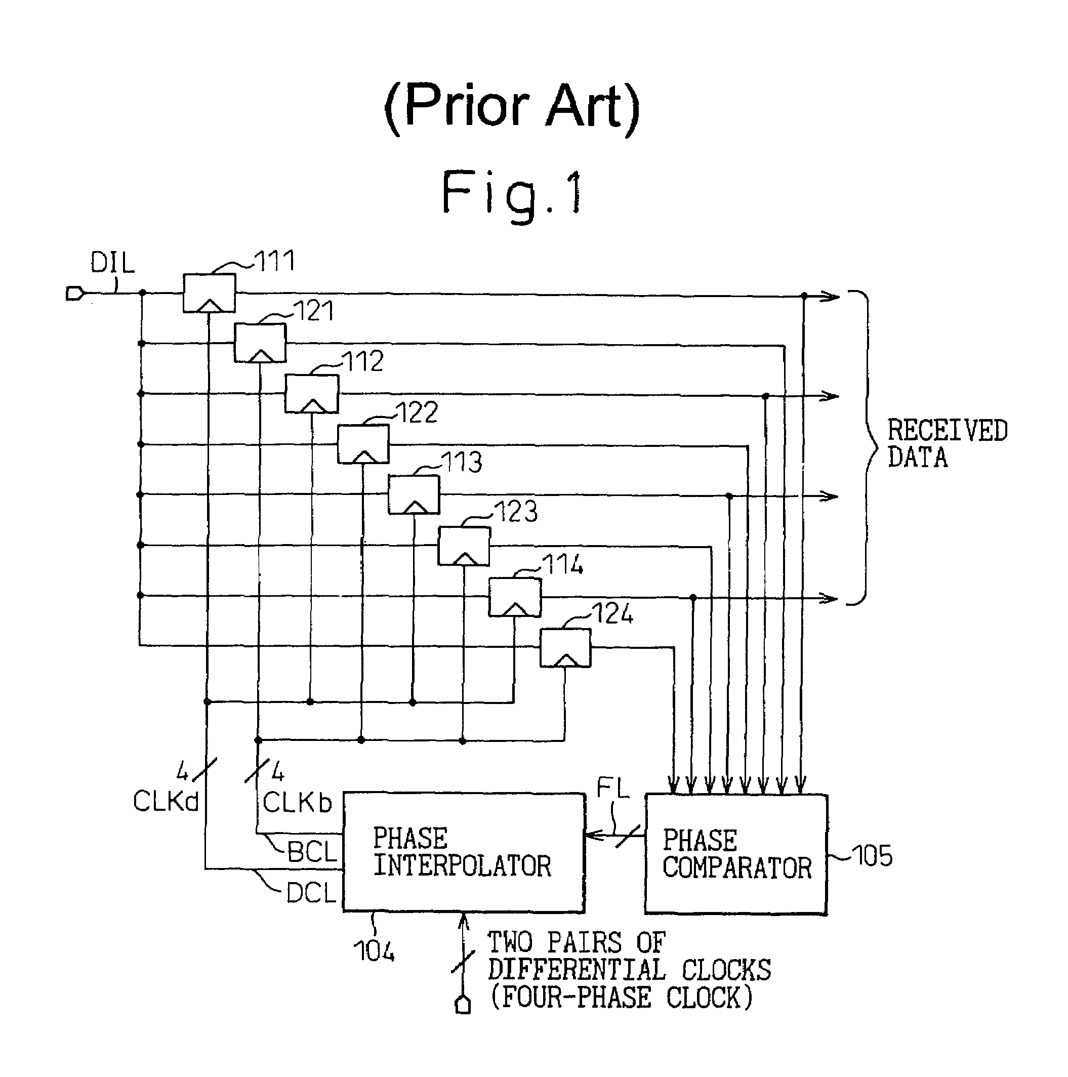
[0104]FIG. 8 is a block diagram schematically showing a receiver circuit according to the present invention, wherein the circuit is configured as a 4-way×2 type interleaving circuit. In FIG. 8, reference numerals 11 to 14 are data detection units, 21 to 24 are boundary detection units, 31 to 34 are boundary skew generating units (buffer delay circuits), 4 is a clock signal generating circuit, and 5 is a phase comparator. Further, reference character DIL is a data input line, DCL is a data detection clock line, BCL is a boundary detection clock line, and FL is a feedback line.

[0105]As shown in FIG. 8, similarly to the earlier described prior art receiver circuit, the receiver circuit (clock recovery circuit) of the first embodiment comprises four data detection units 11 to 14 and four boundary detection units 21 to 24, and the data detection units 11 to 14 and boundary detection units 21 to 24 perform interleaving. Here, the clock CLKd consists of four data detection unit control sig...

second embodiment

[0123]In the second embodiment, a digitally expressed external modulating code is applied to the modulating DAC 45 for conversion into a current, and the output current of the modulating DAC 45 is supplied to the mixer circuit 47, thereby providing a skew to the boundary clock signal (boundary detection clock). As the modulating code supplied to the modulating DAC 45 is digitally expressed, a programmable skew can be generated and, with this skew, the boundary detection timing can be effectively shifted forward or backward relative to the original boundary position.

third embodiment

[0124]FIG. 13 is a block diagram schematically showing a receiver circuit according to the present invention, and FIG. 14 is a block diagram showing one configuration example of a boundary detection / discrimination clock buffer (boundary detection clock buffer) in the receiver circuit of FIG. 13.

[0125]As shown in FIG. 13, the clock signal generating circuit 4 in the receiver circuit (clock recovery circuit) of the third embodiment comprises a clock signal generator 400 and clock buffers 401 and 402. Data detection clocks CLKd (CLKd1 to CLKd4) are supplied to the respective data detection units 11 to 14 via the data detection clock buffer 401, while boundary detection clocks CLKb (CLKb1 to CLKb4) are supplied to the respective boundary detection units 21 to 24 via the boundary detection clock buffer 402.

[0126]As shown in FIG. 14, the boundary detection clock buffer 402 receives the four-phase clock from the clock signal generator 400, and generates the boundary detection clocks CLKb (...


PUM


Abstract

A clock recovery circuit has a boundary detection/discrimination circuit to detect and discriminate a boundary in an input signal in accordance with a first signal. The clock recovery circuit performs clock recovery by controlling the timing of the first signal in accordance with the detected boundary, wherein boundary detection timing in the boundary detection/discrimination circuit is varied by controlling the first signal.

Description

BACKGROUND OF THE INVENTION[0001]1. Field of the Invention[0002]The present invention relates to a technology for enabling high-speed transmission of signals between a plurality of LSI chips or a plurality of devices or circuit blocks within a single chip, or between a plurality of boards or a plurality of cabinets, and more particularly, to a receiver circuit and a clock recovery circuit that uses a feedback loop type clock signal generating circuit.[0003]2. Description of the Related Art[0004]Recently, the performance of components used in computers and other information processing apparatuses has been greatly improved. In particular, dramatic improvements have been made, for example, in the performance of processors and semiconductor memory devices such as DRAMs (Dynamic Random Access Memories). The improvements in the performance of semiconductor memory devices, processors, and the like have reached the point where system performance cannot be improved further unless the speed o...

Claims


Application Information

Patent Timeline
IPC IPC(8): H04L25/00H03L7/06G11C7/10H03L7/081H03L7/091H04L7/033
CPCG11C7/1078G11C7/1087G11C7/222H03L7/0812H03L7/091H04L7/033H04L7/0337
Inventor SAZE, TAKUYATAMURA, HIROTAKACHIBA, TAKAYAGOTOH, KOHTAROHISHIDA, HIDEKI
Owner FUJITSU LTD
Why Eureka
Try Eureka