Smart capture for ATPG (automatic test pattern generation) and fault simulation of scan-based integrated circuits

a technology of automatic test pattern generation and intelligent capture, applied in the direction of error detection/correction, instruments, measurement devices, etc., can solve the problems of large number of test patterns, long test time, and inability to apply capture clocks of different clock domains at the same time during capture operation and simulation, so as to improve the efficiency of an improve the accuracy of the fault simulation, and improve the effect of the efficiency of the existing multiple timeframe handling solution

Inactive Publication Date: 2006-10-17
SYNTEST TECH
View PDF12 Cites 31 Cited by
  • Summary
  • Abstract
  • Description
  • Claims
  • Application Information

AI Technical Summary

Benefits of technology

[0015]The purpose of clock grouping in the present invention is to conduct circuit expansion on the combinational logic blocks related to the grouped clocks. The present invention comprises any method that identifies those clocks which, when grouped together and for which circuit expansion is conducted, will best improve the performance of ATPG and fault simulation.(c) Clock Domain Merging
[0016]The present invention comprises any method that merges a set of clock domains together. For example, suppose that one clock domain CD1 interacts to another clock domain CD2 through a cross-clock domain logic block CCD12. Also suppose that CD1 is captured before CD2. Merging CD1 and CD2 together means that two-time frames will be used for circuit transformation related to the two clock domains and their corresponding cross-clock domain logic blocks. The benefits are as follows: Even the clock domain CD2 is captured after the clock domain CD1 is captured, the controllability of the cross-clock domain logic block CCD12 is still high since the clock domain CD1 is also transformed to obtain the values in the clock domain CD1 after it is captured. As a result, all faults in the cross-clock domain logic block CCD12 can be detected or located. The benefit of clock domain grouping is that it can reduce the number of necessary ordered sequences of capture clocks.(d) Domain-Interconnect Graph Based Capture Order Selection
[0018]As a summarized in BACKGROUND and detailed in U.S. Pat. No. 6,195,776 by Ruiz et al. (2001), prior-art #2 simulates all capture clocks in parallel by selectively setting unknown (X) values on different logic paths, depending on the clock order. The present invention comprises any method that generalizes this unknown-value based method into a constrained-value method. This is achieved by allowing the constraining of a cross-clock domain logic block with logic values, 1 and 0, as well as unknown-values, X's, to force an ATPG program to generate patterns where the cross-clock domain logic block does not change its state during a capture operation. As a result, a fault simulator can perform an accurate fault simulation of patterns where the cross-clock domain logic remains in a constant state during a capture operation. This further improves the accuracy of the fault simulation and ATPG of the unknown-value method. Therefore, a smaller test pattern set and greater measured fault coverage can be achieved.
[0019]To summarize, the present invention uses a hybrid approach for ATPG and fault simulation based on circuit expansion, which is supported by automatic clock grouping and capture order selection. In addition, the present invention uses a new technique to improve the efficiency of an existing multiple timeframe handling solution for ATPG and fault simulation. In conclusion, the present invention provides an efficient solution to ATPG and fault simulation for testing complicated and large-scale scan-based integrated circuits or circuit assemblies by achieving high fault coverage for stuck-at faults, bridging faults, IDDQ faults, transition faults launched from capture, transition faults launched from shift, path-delay faults launched from capture, and path-delay faults launched from shift, with lower memory usage and a smaller number of test patterns.

Problems solved by technology

This makes it impossible to apply the capture clocks of different clock domains simultaneously during the capture operation and simulate the results, since the clock skew between different clock domains would result in incorrect values being captured into some scan cells in the event-based simulation.
The main disadvantage of this method is that a large number of test patterns are required to test the circuit, since only one clock domain can be tested in any given pattern.
This further results in longer test time and larger test data volume, which increases the total test cost.
The main disadvantage of this approach is that the test size is still large, since the ATPG and fault simulator are pessimistic in calculating the fault coverage of different scan test patterns due to the unknown values.
In practice, this is difficult to perform, since it results in a dramatic increase in CPU time requirements.
In practice, the number of clocks that can be applied is limited, resulting in a sub-optimal set of test patterns using longer CPU time.
Furthermore, this is accomplished with a realistic increase in memory size, as opposed to an unrealistic increase in CPU time as in prior-art #3.
The main disadvantage of this approach is that the increase in memory size might prevent the circuit from being able to fit within a given system memory, and might become un-reasonable as design size continues to grow.

Method used


Image

  • Smart capture for ATPG (automatic test pattern generation) and fault simulation of scan-based integrated circuits
  • Smart capture for ATPG (automatic test pattern generation) and fault simulation of scan-based integrated circuits
  • Smart capture for ATPG (automatic test pattern generation) and fault simulation of scan-based integrated circuits

Examples


first embodiment

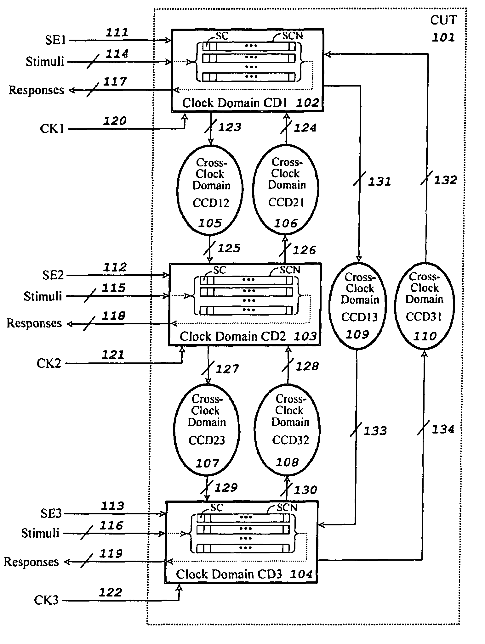
[0120]FIG. 7A shows the domain-interconnect graph used to represent the relationship among the clock domains shown in FIG. 1, with clock grouping in the present invention. 3 nodes are used to represent the 3 clock domains, CD1102 to CD3104. The corresponding scan clocks, CK1120 to CK3122, are also shown in the nodes for easy comprehension. The directed edge between two nodes represents a cross-clock domain block. For example, the edge 701 represents the cross-clock domain block CCD12105 as shown in FIG. 1. In addition, there are two clock groups. One consists of two scan clocks, CK1120 and CK2121, as well as the corresponding clock domains, CD1102 and CD2103. The other consists of one scan clock CK3122 and its corresponding clock domain, CD3104.

[0121]FIG. 7B shows the scan clock waveforms in ATPG (automatic test pattern generation) and fault simulation and FIG. 7C shows the scan clock waveforms in actual test application, both for detecting or locating stuck-at faults, bridging faul...

second embodiment

[0125]FIG. 8A shows the domain-interconnect graph used to represent the relationship among the clock domains shown in FIG. 1, with clock grouping in the present invention. The meanings of nodes, edges, and clock groups are the same as explained in FIG. 7A.

[0126]FIG. 8B shows the scan clock waveforms in ATPG (automatic test pattern generation) and fault simulation and FIG. 8C shows the scan clock waveforms in actual test application, both for detecting or locating stuck-at faults, bridging faults, or IDDQ faults, (referred to as faults) with regard to clock grouping in a second embodiment of the present invention.

[0127]This embodiment requires that all scan clocks be grouped into a set of clock groups and that the clock groups be activated one by one in a selected order during each capture operation. In addition, the capture pulse delays between each clock group should be larger than the possible corresponding clock skew. Furthermore, if a clock group contains multiple scan clocks, t...

third embodiment

[0130]FIG. 9A shows the domain-interconnect graph used to represent the relationship among the clock domains shown in FIG. 1, with clock grouping in the present invention. The meanings of nodes, edges, and clock groups are the same as explained in FIG. 7A.

[0131]FIG. 9B shows the scan clock waveforms in ATPG (automatic test pattern generation) and fault simulation and FIG. 9C shows the scan clock waveforms in actual test application, both for detecting or locating stuck-at faults, bridging faults, or IDDQ faults, (referred to as faults) with regard to clock grouping in a third embodiment of the present invention.

[0132]This embodiment requires that all scan clocks be grouped into a set of clock groups and that the clock groups be activated one by one in a selected order during each capture operation. In addition, the capture pulse delays between each clock group should be larger than the possible corresponding clock skew. Furthermore, if a clock group contains multiple scan clocks, th...


PUM


Abstract

A method for generating stimuli and test responses for testing faults in a scan-based integrated circuit in a selected scan-test mode or a selected self-test mode, the scan-based integrated circuit containing a plurality of scan chains, N clock domains, and C cross-clock domain blocks, each scan chain comprising multiple scan cells coupled in series, each clock domain having one capture clock, each cross-clock domain block comprising a combinational logic network. The method comprises compiling the scan-based integrated circuit into a sequential circuit model; specifying input constraints on the scan-based integrated circuit during a shift and capture operation; specifying a clock grouping to map the N clock domains into G clock domain groups, where N>G>1; transforming the sequential circuit model into an equivalent combinational circuit model according to the input constraints and the clock grouping; and generating the stimuli and test responses on the equivalent combinational circuit model according to the input constraints.

Description

RELATED APPLICATION DATA[0001]This application claims the benefit of U.S. Provisional Application No. 60 / 442,901 filed May 23, 2003, titled “Smart ATPG (Automatic Test Pattern Generation) for Scan-Based Integrated Circuits”, which is hereby incorporated by reference.FIELD OF THE INVENTION[0002]The present invention generally relates to the field of scan-based design and test using design-for-test (DFT) techniques. Specifically, the present invention relates to the field of Scan / ATPG (automatic test pattern generation), Logic BIST (built-in self-test), and Compressed Scan / ATPG.BACKGROUND OF THE INVENTION[0003]In this specification, the term “integrated circuit” is used to describe a chip or MCM (multi-chip module) embedded with DFT (design-for-test) techniques.[0004]An integrated circuit or circuit assembly generally contains multiple clocks, which are either generated internally or supplied externally. Each clock is distributed to a set of storage elements via a skew-minimized netwo...

Claims


Application Information

Patent Timeline
Patent Type & Authority Patents(United States)
IPC IPC(8): G06F11/00G01R31/28G01R31/30G01R31/3183G01R31/3185
CPCG01R31/318342G01R31/318364G01R31/318563G01R31/318594G01R31/3008
Inventor WANG, LAUNG-TERNGABDEL-HAFEZ, KHADER S.WEN, XIAOQINGSHEU, BORYAU JACKWANG, SHUN-MIIN
Owner SYNTEST TECH
Why Eureka
Try Eureka