Multicrystalline silicon substrate and process for roughening surface thereof

Active Publication Date: 2006-10-31
KYOCERA CORP
View PDF5 Cites 43 Cited by
  • Summary
  • Abstract
  • Description
  • Claims
  • Application Information

AI Technical Summary

Benefits of technology

[0023]This process allows fine textures to be formed uniformly, thereby effectively reducing reflectance in the

Problems solved by technology

However, they have the disadvantage of high production cost of the substrates.
In contrast, multicrystalline silicon solar cells have the disadvantage of inferior substrate quality making it difficult to improve conversion efficiency, while they have the advantage of low production cost.
However, when fabricating a solar cell using a multicrystalline substrate, since texture etching with an alkaline aqueous solution depends on the crystal orientation, such a pyramidal pattern cannot be formed uniformly.
For this reason, this poses the problem that the overall reflectance cannot be reduced effectively.
Silicon substrates fabricated by such a process include a layer that is mechanically damaged by the slicing remaining on the surface, which causes degradat

Method used


Image

  • Multicrystalline silicon substrate and process for roughening surface thereof
  • Multicrystalline silicon substrate and process for roughening surface thereof
  • Multicrystalline silicon substrate and process for roughening surface thereof

Examples


Embodiment Construction

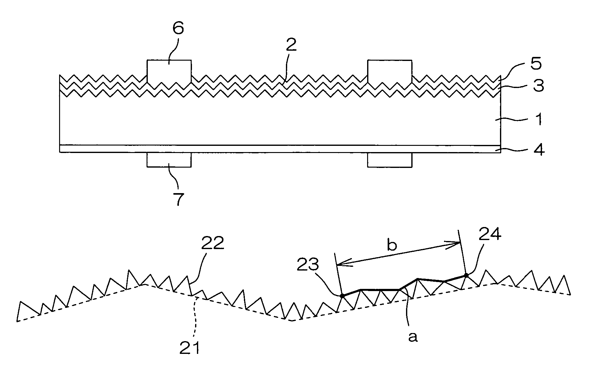
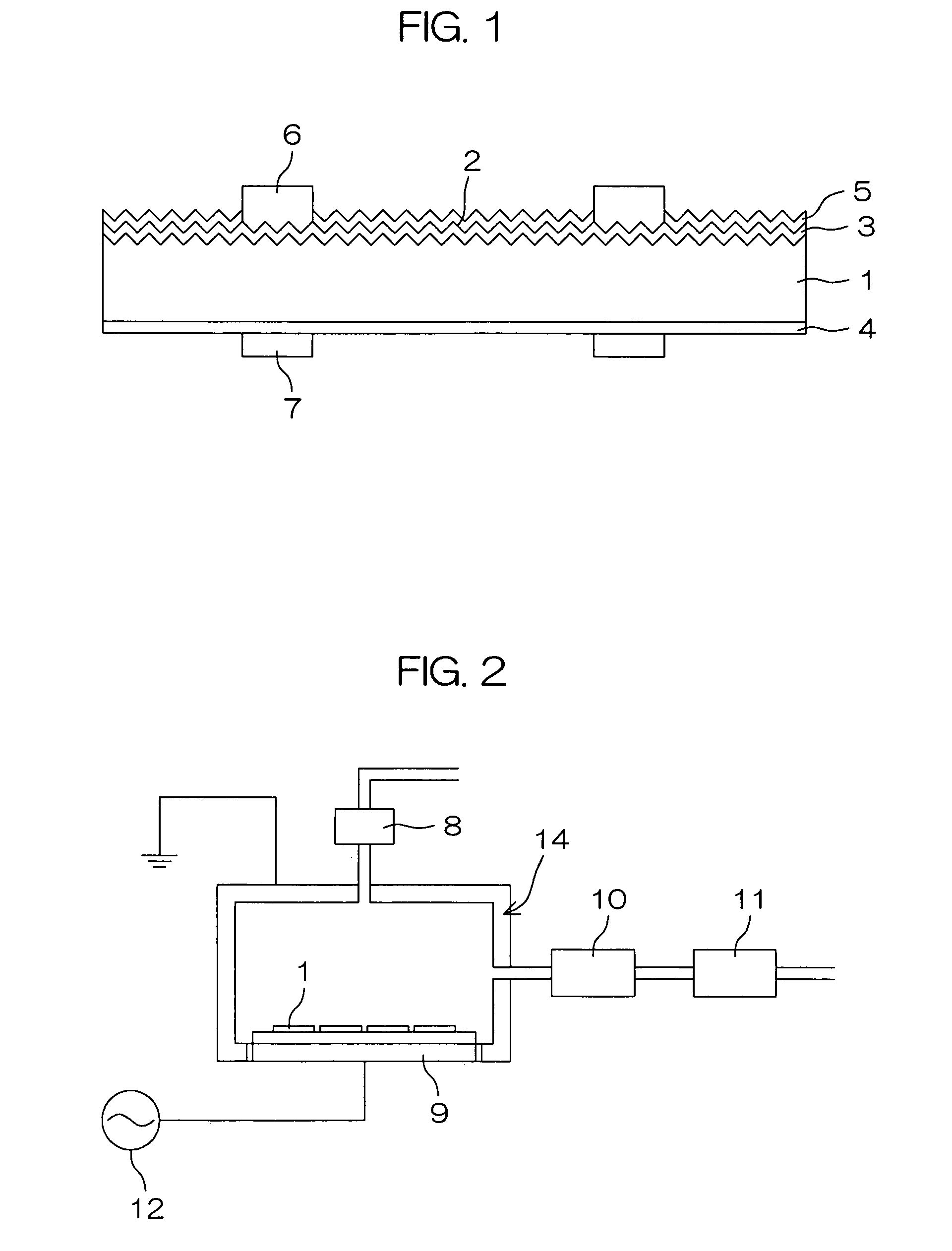
[0031]A specific embodiment of the present invention will be hereinafter described in detail with reference to the accompanying drawings taking a bulk crystalline silicon solar cell as an example. However, the present invention is not limited to this example and applicable to solar cells of other types including thin film solar cells using a glass substrate.

[0032]FIG. 1 is a cross section showing a structure of a solar cell fabricated by a substrate processing method of the invention. Referring to FIG. 1, numeral 1 denotes a silicon substrate, numeral 2 denotes textures formed on the silicon substrate 1, numeral 3 denotes an impurity diffusing layer on the light-reception surface side, numeral 4 denotes an impurity diffusing layer (BSF) on the back surface side of the silicon, numeral 6 denotes a surface electrode, and numeral 7 denotes a back surface electrode.

[0033]On the surface side of the silicon substrate 1, impurity diffusing layer 3 in which another type impurity against the...


PUM

PropertyMeasurementUnit
Widthaaaaaaaaaa
Heightaaaaaaaaaa
Ratioaaaaaaaaaa

Abstract

A surface of a multicrystalline silicon substrate is etched with an alkaline aqueous solution in a condition so that a surface area-to-planar surface area ratio R is smaller than 1.1. A multiplicity of fine textures are formed over the irregularities by dry etching. This allows fine textures to be formed uniformly, and a solar cell with high efficiency can thus be produced.

Description

[0001]This application is based on application No. 2003-019535 filed in Japan, the content of which is incorporated hereinto by reference.BACKGROUND OF THE INVENTION[0002]1. Field of the Invention[0003]The present invention relates to a multicrystalline silicone substrate and a process for roughening surface thereof, preferably used in a field of solar cell or the like.[0004]2. Description of the Related Art[0005]Solar cell is a device that converts light energy incident on its surface such as sunlight into electric energy. Various approaches have been attempted in order to improve efficiency in converting light energy into electric energy. One of such approaches is technique that reduces reflectance of light incident on the surface of the substrate. Reducing the reflectance of light incident on the surface allows the conversion efficiency into electric energy to be improved.[0006]The main types of solar cells are classified by material used into crystalline silicon solar cells, amo...

Claims


Application Information

Patent Timeline
IPC IPC(8): B32B9/04B44C1/22H01L31/00C01B33/02H01L21/306H01L21/3065H01L31/0236H01L31/04H01L31/068
CPCH01L21/30604H01L31/0236H01L31/068Y10T428/24355Y02E10/547H01L31/02363Y02E10/546
Inventor INOMATA, YOSUKE
Owner KYOCERA CORP
Why Eureka
Try Eureka