Method and apparatus for forming substrate for semiconductor or the like

Inactive Publication Date: 2006-10-31
ADVANCED LCD TECH DEVMENT CENT
View PDF4 Cites 5 Cited by
  • Summary
  • Abstract
  • Description
  • Claims
  • Application Information

AI Technical Summary

Benefits of technology

[0013]It is an object of the present invention to provide a method and an apparatus which detect a st

Problems solved by technology

For example, a time of melting, a reflection factor or a transmittance is obtained from this one set of information, and it is thus difficult to determine important optical characteristics of the thin film such as a refractive index or an extinction coefficient in order to evaluate a degree of progress that the thin film is crystallized.
Further, it is substantially impossible to measure a change in the reflected light intensity concerning a melting-solidification process of several-hundred ns, i.e., a degree of progress that the thin film is crystallized with a time resolution higher than 1 ns.
Therefore, the characteristics of the thin film cannot be correctly specified in the prior art, and there is known that a defect of, e.g., electrical characteristics is generated in a liquid crystal display apparatus or the like using as a switching element a thin film transistor having an unsurely evaluated thin film.

Method used


Image

  • Method and apparatus for forming substrate for semiconductor or the like
  • Method and apparatus for forming substrate for semiconductor or the like
  • Method and apparatus for forming substrate for semiconductor or the like

Examples


Embodiment Construction

[0036]An embodiment according to the present invention will now be described hereinafter with reference to the accompanying drawings.

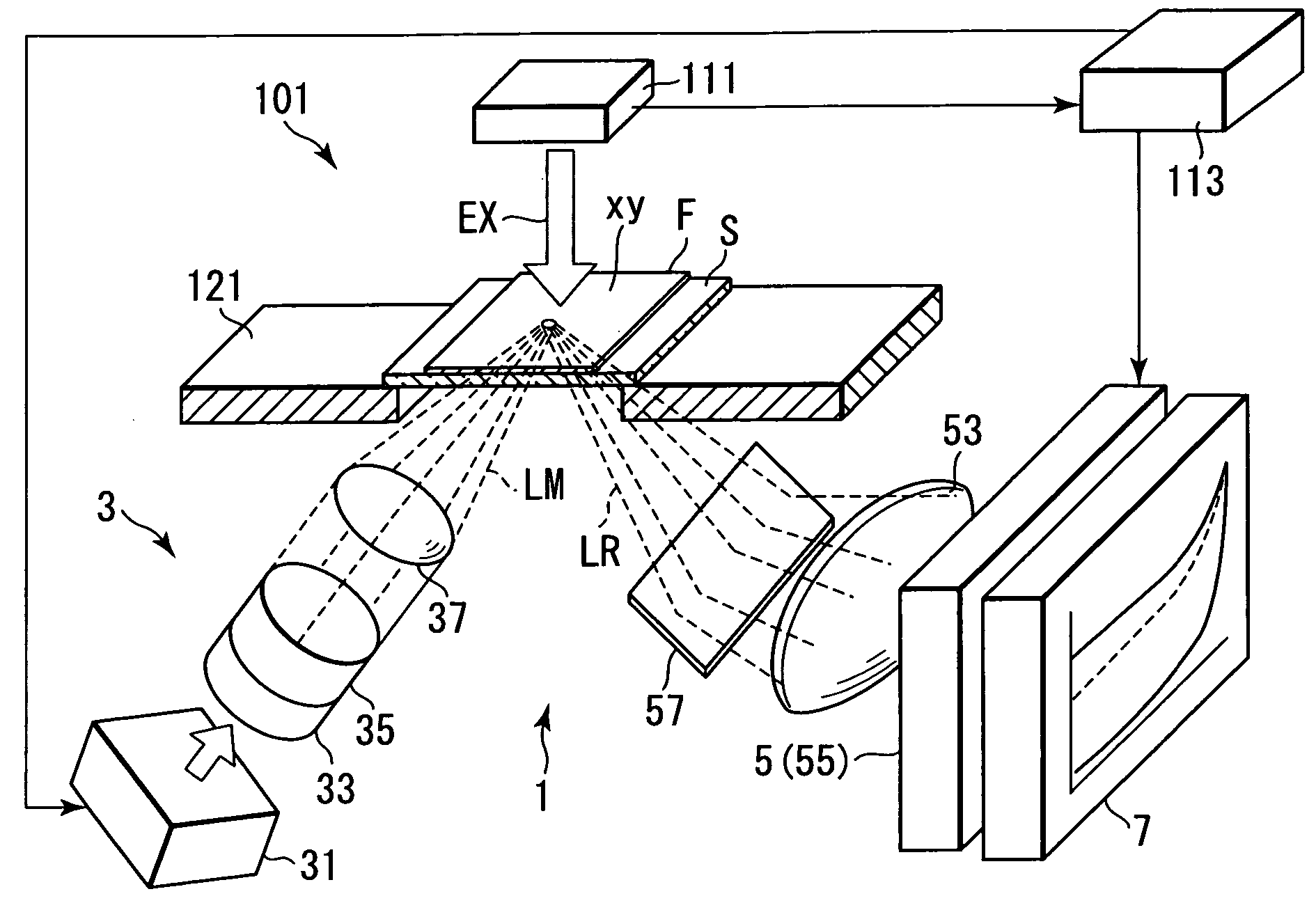
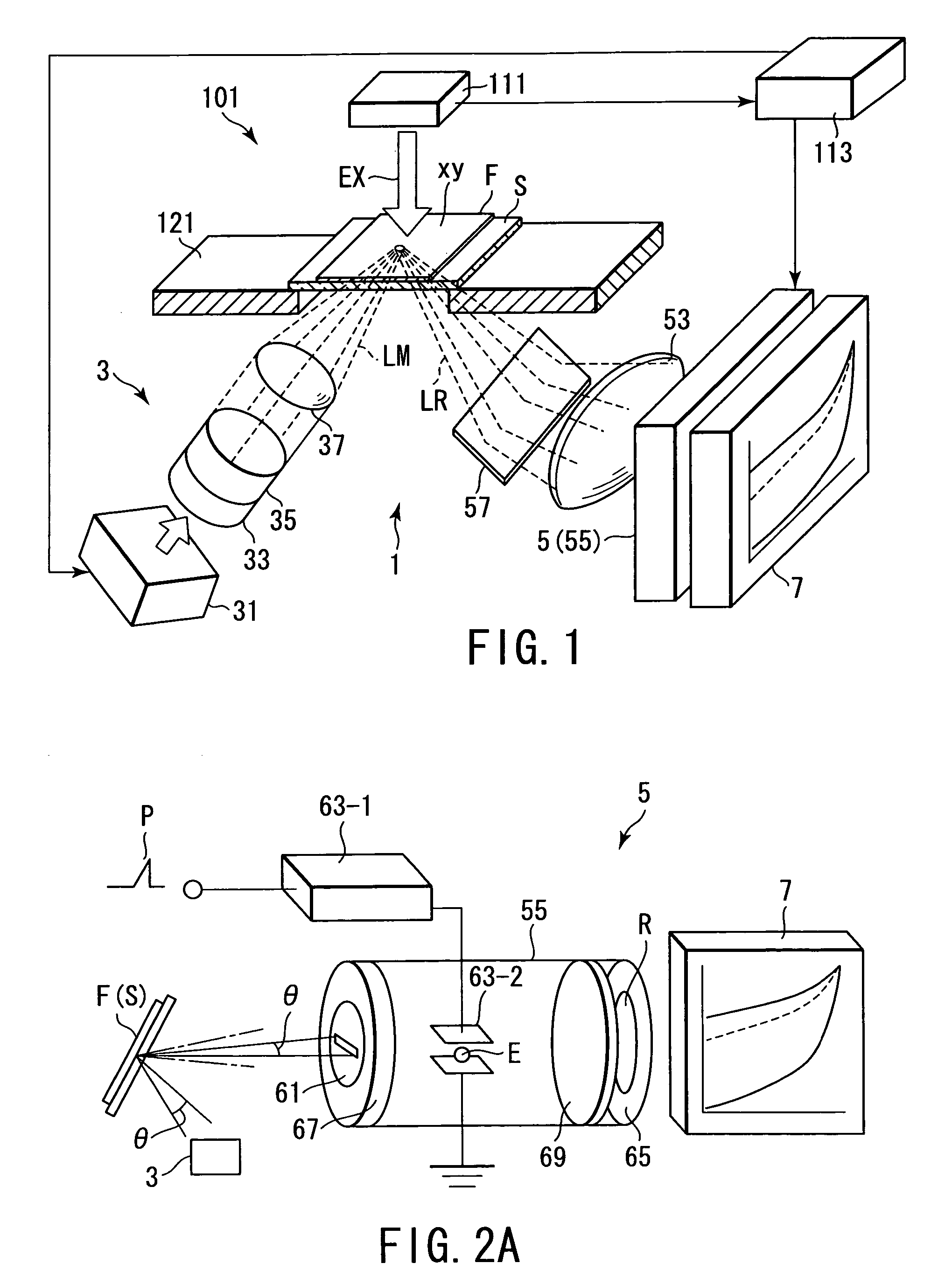
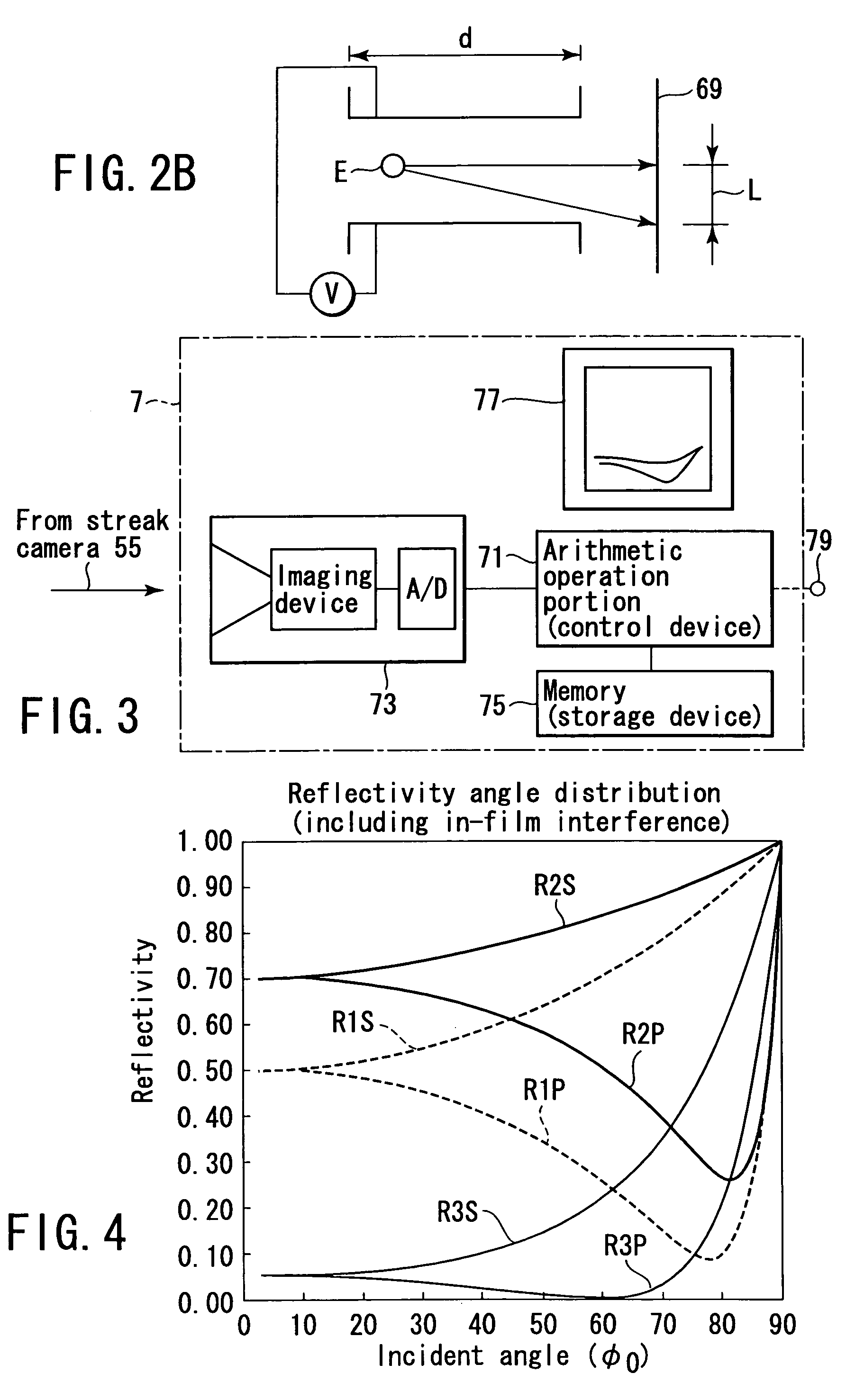
[0037]FIG. 1 shows an example of a laser annealing apparatus as an example of a substrate finishing / processing apparatus in which an apparatus which determines characteristics of a semiconductor thin film according to an embodiment of the present invention is incorporated.

[0038]The apparatus 1 which determines characteristics of a semiconductor thin film is integrally incorporated at a predetermined position of, e.g., a laser annealing apparatus 101 which is an example of a substrate finishing / processing apparatus holding a substrate S as a target whose characteristics should be determined for finishing / processing, which is a rear surface side of the substrate S in the example of FIG. 1. It is to be noted that each of the apparatus 1 which determines characteristics of the thin film and the laser annealing apparatus 101 is operated in a vacuum containe...


PUM


Abstract

In an apparatus which determines characteristics of a thin film according to the present invention, a temporal change in a refractive index n and an extinction coefficient k of a thin film in a period from start of a change in the thin film as a processing target (e.g., melting) to end of the change (e.g., solidification) can be obtained with a high time resolution of pico-seconds. Based on this, it is possible to know a progress of a change in state of the thin film (e.g., crystallization) or a transition of growth of crystal grains in units of pico-seconds.

Description

CROSS-REFERENCE TO RELATED APPLICATIONS[0001]This application is based upon and claims the benefit of priority from the prior Japanese Patent Application No. 2002-341330, filed Nov. 25, 2002, the entire contents of which are incorporated herein by reference.BACKGROUND OF THE INVENTION[0002]1. Field of the Invention[0003]The present invention relates to a method and an apparatus for determining characteristics of a semiconductor thin film.[0004]2. Description of the Related Art[0005]For example, in regard to manufacture of a thin film transistor for a switching element of, e.g., a liquid crystal display apparatus or an organic electroluminescence display apparatus, M. Hatano, S. Moon, M. Lee and K. Suzuki, (C. P. Grigoropoulos), Journal of Applied Physics, vol. 87, No. 1, 2000, pp, 36 to 43, Excimer Laser-Induced Temperature Field in Melting and Resolidification of Silicon Thin Films reports a method by which an annealed position provided to an amorphous silicon thin film is irradiat...

Claims


Application Information

Patent Timeline
IPC IPC(8): G01J4/00G01N21/21G01N21/84
CPCG01N21/211G01N21/8422
Inventor TAKAMI, YOSHIO
Owner ADVANCED LCD TECH DEVMENT CENT
Why Eureka
Try Eureka