Stacked capacitor and method for fabricating same

a technology of stacked capacitors and capacitors, applied in the direction of stacked capacitors, fixed capacitors, fixed capacitor details, etc., can solve the problems of physical constraints limiting the expansion of miniaturisation, and achieve the effect of reducing the surface area requirement of capacitors, high capacitance values, and easy realization within an integrated circui

Active Publication Date: 2006-10-31
TEXAS INSTR INC
View PDF14 Cites 5 Cited by
  • Summary
  • Abstract
  • Description
  • Claims
  • Application Information

AI Technical Summary

Benefits of technology

[0003]The invention provides a stacked capacitor consisting of a silicon base plate, a poly-silicon center plate arranged above the base plate, a lower gate-oxide dielectric arranged between the base plate and the center plate, a cover plate made of a metallic conductor and arranged above the center plate, and an upper dielectric arranged between the center plate and the cover plate, the cover plate and the base plate being electrically connected to each other and together forming a first capacitor electrode, the center plate forming a second capacitor electrode. The formation of the stacked capacitor with three plates, where the two outer ones are connected to each other to form a common capacitor electrode, reduces the surface area requirement of the capacitor by half in comparison with a two-plate capacitor. Between the heavily-doped silicon base plate and the poly-silicon center plate, high capacitance values can be achieved as a result of this material combination. All three plates, as well as their intermediate dielectric layers, can be produced without additional resources in one manufacturing process of an integrated semiconductor circuit, since the corresponding layers are already available in this sequence as part of the manufacturing process. The stacked capacitor according to the invention can, therefore, be realized within an integrated circuit very easily and at low cost.

Problems solved by technology

However, physical constraints set limits to increasing miniaturisation.

Method used


Image

  • Stacked capacitor and method for fabricating same
  • Stacked capacitor and method for fabricating same

Examples


Embodiment Construction

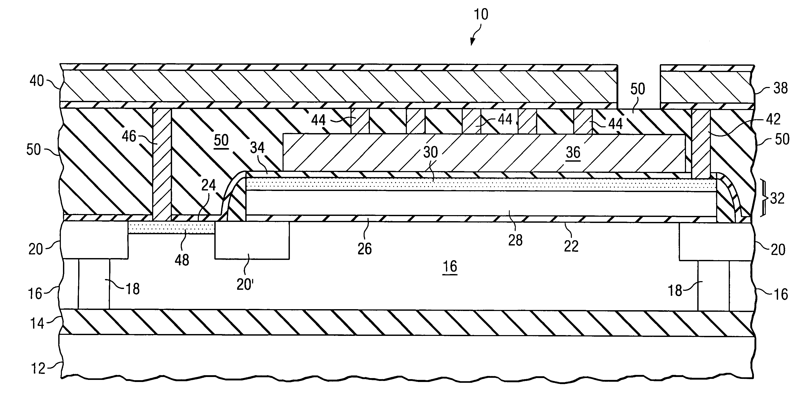
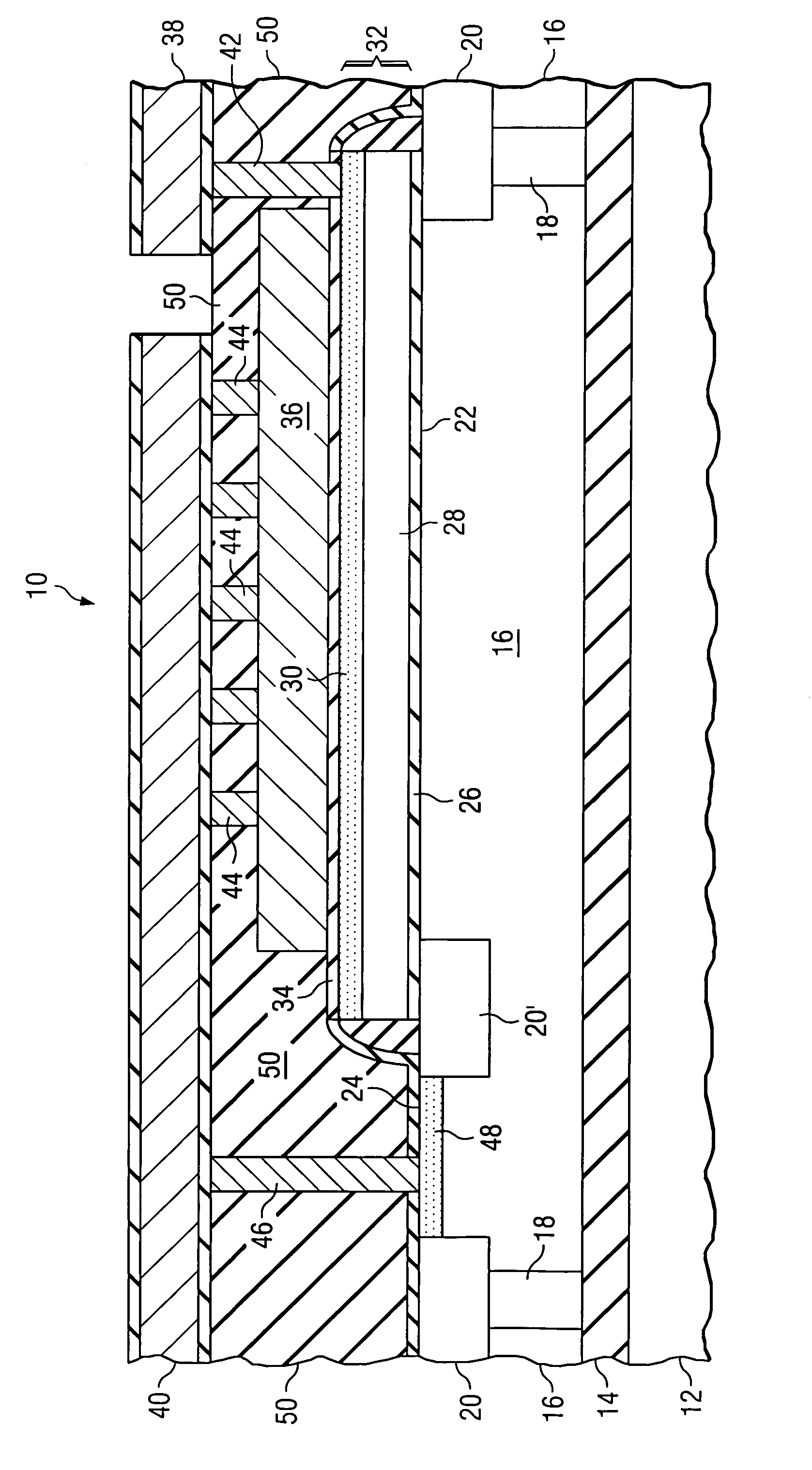
[0016]The stacked capacitor 10 represented in the drawing is an integral part of an integrated circuit, of which the drawing only shows a section that is essential for the description. The integrated circuit is assembled on a silicon substrate 12 that serves as a carrier. A buried oxide layer 14 is formed on the surface of the substrate 12, which serves to insulate the components on upper layers from the substrate 12.

[0017]A buried silicon layer is arranged on top of the oxide layer 14, which forms a base plate 16 for the stacked capacitor 10. The base plate 16 is insulated with respect to adjacent circuit components in a conventional manner by deep and shallow trenches 18 and 20, respectively, which are filled with an insulating substance, such as silicon oxide. The base plate 16 is heavily doped, whereby it may be either n or p doped, depending on which type of doping is available in the production process of the integrated circuit, and which is suitable for the area concerned. Th...


PUM


Abstract

The invention relates to a stacked capacitor (10) comprising a silicon base plate (16), a poly-silicon center plate (32) arranged above the base plate (16), a lower gate-oxide dielectric (26) arranged between the base plate (16) and the center plate (32), a cover plate (36) made of a metallic conductor and arranged above the center plate (32), and an upper dielectric (34) arranged between the center plate (32) and the cover plate (36). The cover plate (36) and the base plate (16) are electrically connected to each other and together form a first capacitor electrode. The center plate (32) forms a second capacitor electrode. The invention further relates to an integrated circuit with such a stacked capacitor, as well as to a method for fabrication of a stacked capacitor as part of a CMOS process.

Description

FIELD OF THE INVENTION[0001]The invention relates to a stacked capacitor, an integrated circuit containing such a stacked capacitor, and a method for fabricating a stacked capacitor as part of a CMOS process.BACKGROUND OF THE INVENTION[0002]The requirement for ever increasing package densities demands that the structure of the individual circuit components must become even smaller. However, physical constraints set limits to increasing miniaturisation. Especially, for capacitors whose capacity depends directly on the plate surface a reduction in surface demands is therefore desirable.SUMMARY OF THE INVENTION[0003]The invention provides a stacked capacitor consisting of a silicon base plate, a poly-silicon center plate arranged above the base plate, a lower gate-oxide dielectric arranged between the base plate and the center plate, a cover plate made of a metallic conductor and arranged above the center plate, and an upper dielectric arranged between the center plate and the cover pl...

Claims


Application Information

Patent Timeline
Patent Type & Authority Patents(United States)
IPC IPC(8): H01G4/00H01L21/02H01L27/06H01L27/08
CPCH01L27/0629H01L27/0805H01L28/40
Inventor BALSTER, SCOTTEL-KAREH, BADIHSTEINMANN, PHILIPPDIRNECKER, CHRISTOPH
Owner TEXAS INSTR INC
Why Eureka
Try Eureka