

Composition for forming porous film, porous film and method for forming the same, interlevel insulator film, and semiconductor device
a technology of porous film and film, which is applied in the direction of solid-state devices, inorganic chemistry, building components, etc., can solve the problems of obstructing continuity, reducing and difficult practical use, so as to improve the mechanical strength of the semiconductor device, reduce the hygroscopic property of the porous film, and improve the stability of the produced coating solution
- Summary
- Abstract
- Description
- Claims
- Application Information
AI Technical Summary
Benefits of technology
Problems solved by technology
Method used
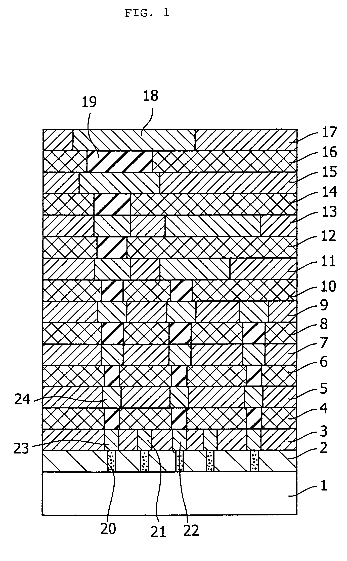
Image

Examples
synthetic example 1
(Synthesis of Siloxane Polymer with Acidic Catalyst)
[0066]An aqueous 0.05 wt % nitric acid solution of 60 g was added to the solution mixture of tetraethoxysilane (80 g), methyltrimethoxysilane (50 g) and ethanol (460 g), and stirred for four hours at 25° C. The ethanolic solution of the silicone polymer was obtained.
synthetic example 2
(Synthesis of Siloxane Polymer with Basic Catalyst)
[0067]A solution of tetraethoxysilane (60 g) and methyltrimethoxysilane (30 g) was added to the mixture of the solution of an aqueous 40 wt % methylamine solution (log), ultra pure water (640 g) and ethanol (1200 g), and stirred for four hours at 75° C. The ethanolic solution of the silicone polymer was obtained.
synthetic example 3
(Synthesis of Siloxane Polymer with Basic Catalyst)
[0068]A solution of tetramethoxysilane (40 g) and methyltrimethoxysilane (30 g) was added to the mixture of an aqueous 28wt % ammonia solution (10 g), ultra pure water (640 g) and ethanol (1200 g), and stirred for four hours at 75° C. The ethanolic solution of silicone polymer was obtained.
PUM
| Property | Measurement | Unit |
|---|---|---|
| relative permittivity | aaaaa | aaaaa |
| relative permittivity | aaaaa | aaaaa |
| diameter | aaaaa | aaaaa |
Abstract
Description
Claims
Application Information