Pattern formation method

a pattern and pattern technology, applied in the field of pattern formation methods, can solve the problems of reducing the productivity and yield of the semiconductor device fabrication process, the shape of the resist pattern, and the inability to use photolithography using a shorter wavelength. the effect of neutralization

Inactive Publication Date: 2006-11-14
RPX CORP
View PDF1 Cites 2 Cited by
  • Summary
  • Abstract
  • Description
  • Claims
  • Application Information

AI Technical Summary

Benefits of technology

[0039]In the fourth pattern formation method, since an acid generated in an unexposed portion is neutralized by a base generated from the compound for generating a base included in the solution owing to heat caused by light energy, the solubility of the unexposed portion in a developer is not changed. On the other hand, since the amount of acid generated in an exposed portion of the resist film from an acid generator is large, even when the base generated from the compound for generating a base included in the solution owing to the heat caused by the light energy neutralizes the acid generated in the exposed portion, the influence of the neutralization is small, and hence, the solubility of the exposed portion in the developer can be definitely changed. Accordingly, the contrast between the exposed portion and the unexposed portion of the resist film can be largely improved, so that the resist pattern can be formed in a good shape.
[0040]Leakage light of the exposing light that enters the unexposed portion of the resist film generates a small amount of acid from the acid generator in a surface portion of the unexposed portion. Therefore, when the pattern exposure is carried out while supplying, onto the resist film, the solution including the compound for generating a base through application of heat as in the fourth pattern formation method, the acid generated from the acid generator in the surface portion of the unexposed portion can be more efficiently neutralized by the base generated from the compound for generating a base through application of heat as compared with the case where the compound for generating a base through application of heat is included in the resist film.

Problems solved by technology

However, since there remain a large number of problems in exposure systems and resist materials, photolithography using exposing light of a shorter wavelength has not been put to practical use.
Although the positive chemically amplified resist material is used in the first or second conventional pattern formation method, also when a negative chemically amplified resist material, the resultant resist pattern is in a defective shape.
When a resist pattern in such a defective shape is used for etching a target film, the resultant pattern is also in a defective shape, which disadvantageously lowers the productivity and the yield in the fabrication process for semiconductor devices.

Method used


Image

  • Pattern formation method
  • Pattern formation method
  • Pattern formation method

Examples


embodiment 1

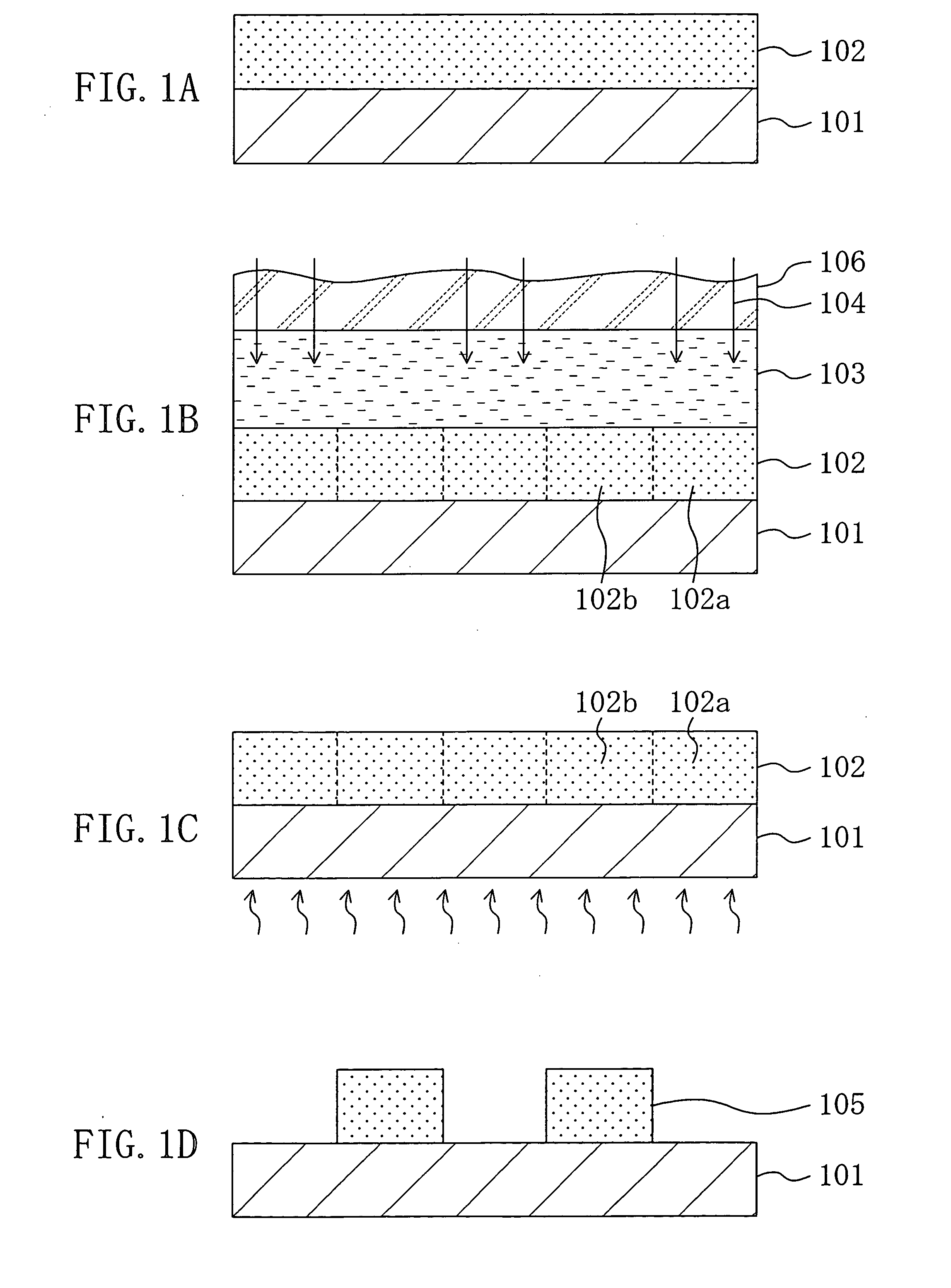
[0052]A pattern formation method according to Embodiment 1 of the invention will now be described with reference to FIGS. 1A through 1D.

[0053]First, a positive chemically amplified resist material having the following composition is prepared:

[0054]Base polymer: poly((styrenehexafluoroisopropylalcohol)-(α-trifluoromethyl t-butylacrylate)) (wherein styrenehexafluoroisopropylalcohol: α-trifluoromethyl t-butylacrylate=40 mol %:60 mol %) . . . 2 g

[0055]Acid generator: triphenylsulfonium triflate . . . 0.08 g

[0056]Solvent: propylene glycol monomethyl ether acetate . . . 20 g

[0057]Next, as shown in FIG. 1A, the aforementioned chemically amplified resist material is applied on a substrate 101 so as to form a resist film 102 with a thickness of 0.35 μm.

[0058]Then, as shown in FIG. 1B, while supplying, onto the resist film 102, a solution 103 of water including 0.01 wt % of triethanolamine (a basic compound), pattern exposure is carried out by irradiating the resist film 102 with exposing lig...

embodiment 2

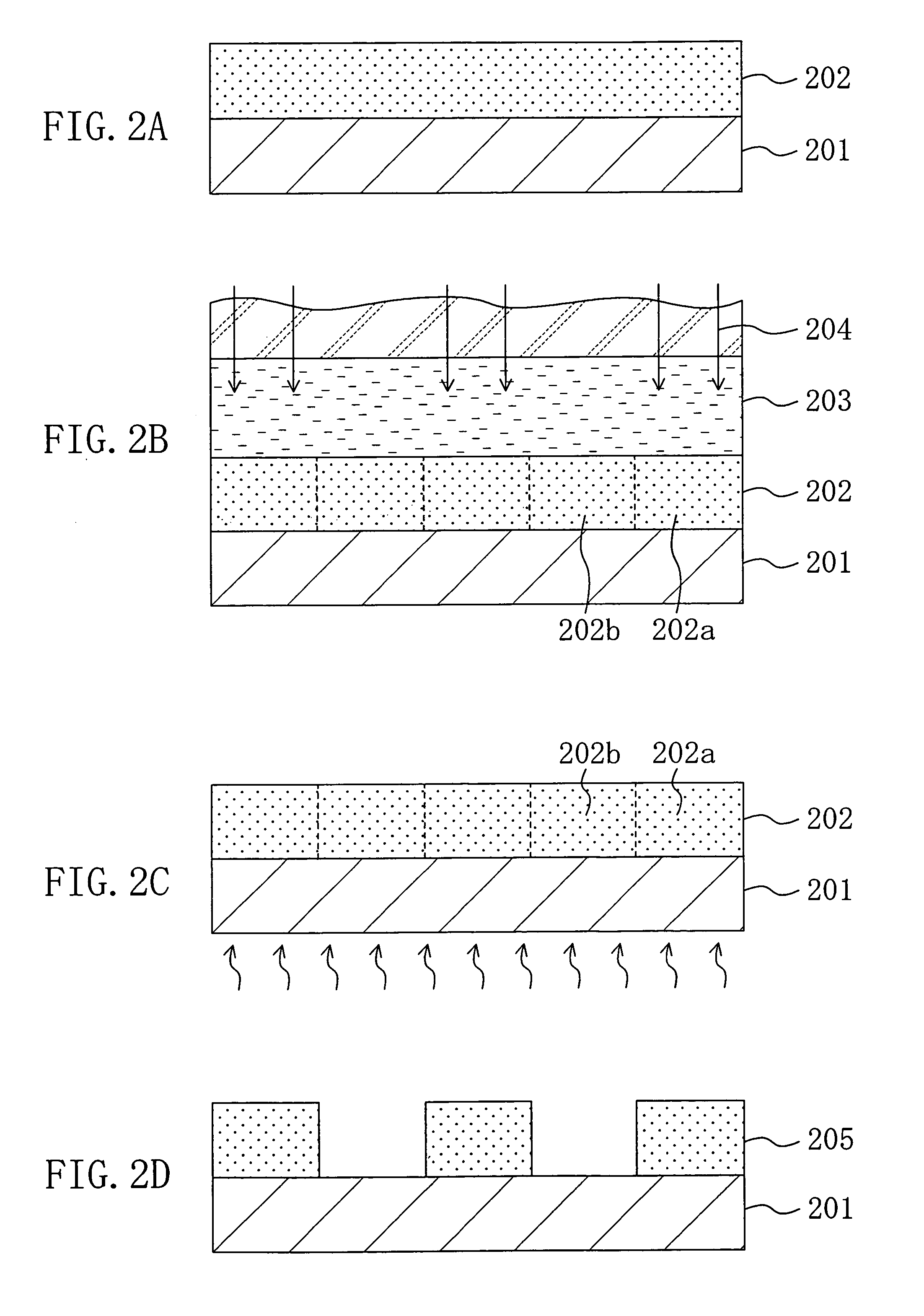
[0061]A pattern formation method according to Embodiment 2 of the invention will now be described with reference to FIGS. 2A through 2D.

[0062]First, a negative chemically amplified resist material having the following composition is prepared:

[0063]Base polymer: poly((styrenehexafluoroisopropylalcohol)-(α-trifluoromethylacrylic acid)) (wherein styenehexafluoroisopropyalchol: α-trifluoromethylacrylic acid=40 mol %:60 mol %) . . . 2 g

[0064]Crosslinking agent: 1,3,5-N-(dimethoxymethyl)melamine . . . 0.7 g

[0065]Acid generator: triphenylsulfonium triflate . . . 0.08 g

[0066]Solvent: propylene glycol monomethyl ether acetate . . . 20 g

[0067]Next, as shown in FIG. 2A, the aforementioned chemically amplified resist material is applied on a substrate 201 so as to form a resist film 202 with a thickness of 0.35 μm.

[0068]Then, as shown in FIG. 2B, while supplying, onto the resist film 202, a solution 203 of water including 0.02 wt % of trimethylamine (a basic compound), pattern exposure is carri...

embodiment 3

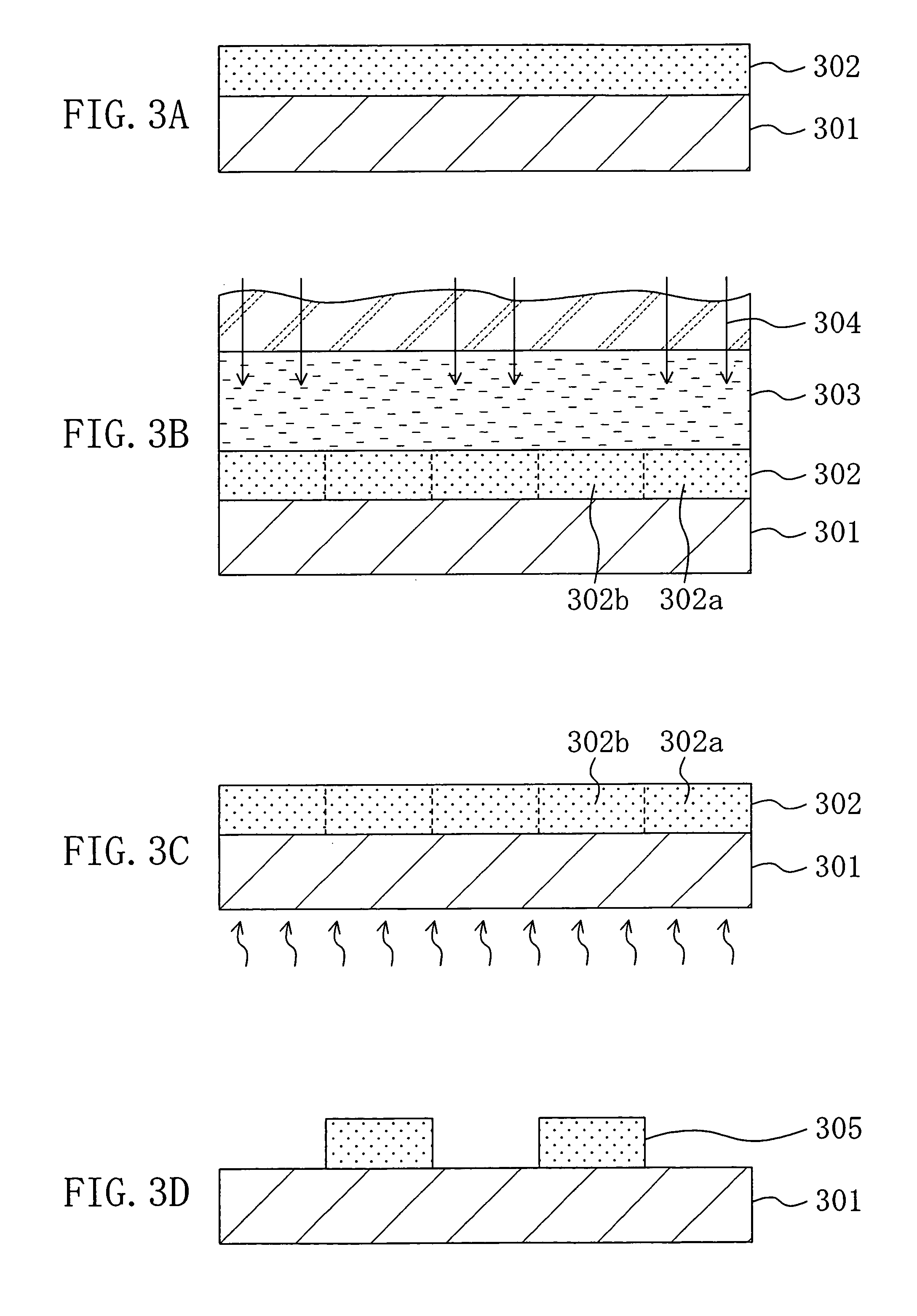
[0088]A pattern formation method according to Embodiment 3 of the invention will now be described with reference to FIGS. 3A through 3D.

[0089]First, a positive chemically amplified resist material having the following composition is prepared:

[0090]Base polymer: poly((styrenehexafluoroisopropylalcohol)-(α-trifluoromethyl t-butylacrylate)) (wherein styrenehexafluoroisopropylalcohol: α-trifluoromethyl t-butylacrylate=40 mol %:60 mol %) . . . 2 g

[0091]Acid generator: triphenylsulfonium triflate . . . 0.08 g

[0092]Solvent: propylene glycol monomethyl ether acetate . . . 20 g

[0093]Next, as shown in FIG. 3A, the aforementioned chemically amplified resist material is applied on a substrate 301 so as to form a resist film 302 with a thickness of 0.20 μm.

[0094]Then, as shown in FIG. 3B, while supplying, onto the resist film 302, a solution 303 of perfluoropolyether (represented by Chemical Formula 1 below) including 0.02 wt % of polyvinylamine (a basic polymer), pattern exposure is carried out...


PUM

PropertyMeasurementUnit
mol %aaaaaaaaaa
thicknessaaaaaaaaaa
temperatureaaaaaaaaaa

Abstract

After forming a resist film of a chemically amplified resist material, pattern exposure is carried out by selectively irradiating the resist film with exposing light while supplying, onto the resist film, a solution including a basic compound. After the pattern exposure, the resist film is subjected to post-exposure bake and is then developed with an alkaline developer. Thus, a resist pattern made of an unexposed portion of the resist film can be formed in a good shape.

Description

BACKGROUND OF THE INVENTION[0001]The present invention relates to a pattern formation method for use in fabrication process and the like for semiconductor devices.[0002]In accordance with the increased degree of integration of semiconductor integrated circuits and downsizing of semiconductor devices, there are increasing demands for further rapid development of lithography technique. Currently, pattern formation is carried out through photolithography using exposing light of a mercury lamp, KrF excimer laser, ArF excimer laser or the like, and use of F2 laser lasing at a shorter wavelength is being examined. However, since there remain a large number of problems in exposure systems and resist materials, photolithography using exposing light of a shorter wavelength has not been put to practical use.[0003]In these circumstances, immersion lithography has been recently proposed for realizing further refinement of patterns by using conventional exposing light (M. Switkes and M. Rothschi...

Claims


Application Information

Patent Timeline
Patent Type & Authority Patents(United States)
IPC IPC(8): G03F7/20G03F7/38G03F7/00G03F7/004G03F7/038G03F7/039H01L21/027
CPCG03F7/0046G03F7/0382G03F7/0392G03F7/2041
Inventor ENDO, MASAYUKISASAGO, MASARU
Owner RPX CORP
Why Eureka
Try Eureka