Integrated optical element

a technology of optical elements and optical elements, applied in the direction of optical waveguide light guides, instruments, nanotechnology, etc., can solve the problems of inability to realize crystal axes with different directions at optional locations in a single crystal, and inability to make a transmitted polarized light have the dependency on location

Inactive Publication Date: 2006-11-14
PHOTONIC LATTICE
View PDF2 Cites 27 Cited by
  • Summary
  • Abstract
  • Description
  • Claims
  • Application Information

AI Technical Summary

Benefits of technology

[0020]An example of a method for realizing a photonic crystal is the self-cloning method (Japanese Patent Laid-Open Publication No.Hei 10-335,758). This is a method for performing a layer deposition while keeping a corrugated shape reflecting the pattern of a substrate by depositing an alternate multilayer film on the substrate with a corrugated pattern formed on it by the use of a film forming method using both diffuse incidence and sputter etching of deposited particles represented by the bias sputtering method. This mechanism can be explained as superposition of the following three effects at a proper ratio: (1) an effect that the deposition rate of particles in a depression shaded due to dispersion incidence is reduced, (2) an effect that the etching rate by a sputter etching process of a face inclined at an angle of about 50 to 60 degrees is maximum, and (3) an effect that particles shaved off by a sputter etching process stick again to another location on a substrate (“Mechanism of Forming a Three-Dimensionally Periodical Nano-Structure Made by the Bias Sputtering Method” by Shojiro Kawakami, Hisashi Sato and Takayuki Kawashima, Journal of Institute of Electronics, Information and Communication Engineers C-1, Vol. J81-C-1, No.2, pp.108-109, February, 1998).

Problems solved by technology

Therefore, in case of either amorphous materials or crystalline materials, realizing different optical characteristics in a single optical element has only been possible by combining different materials with one another by means of an adhesive agent and the like.
This provides an inexpensive and large-area polarizer but has a disadvantage of being low in extinction ratio and inferior in temperature characteristic.
Since a drawing process is used for any one of the above-mentioned polarizers, it is impossible to make a transmitted polarized light have the dependency on location.
Since they each use a natural crystal, its crystal axes are specifically determined and it is impossible to realize crystal axes with different directions at optional locations in a single crystal.
Therefore, in case of attempting to make its polarization characteristic have the dependency on location, it is necessary to arrange a plurality of multilayer films in different directions, and it is apparent that this cannot be realized by means of a single element.
Therefore, the material itself is expensive and a high-accuracy thickness control is required for making a wave plate act as a ¼-wavelength plate or a ½-wavelength plate.

Method used


Image

  • Integrated optical element
  • Integrated optical element
  • Integrated optical element

Examples


embodiment 1

(Embodiment 1)

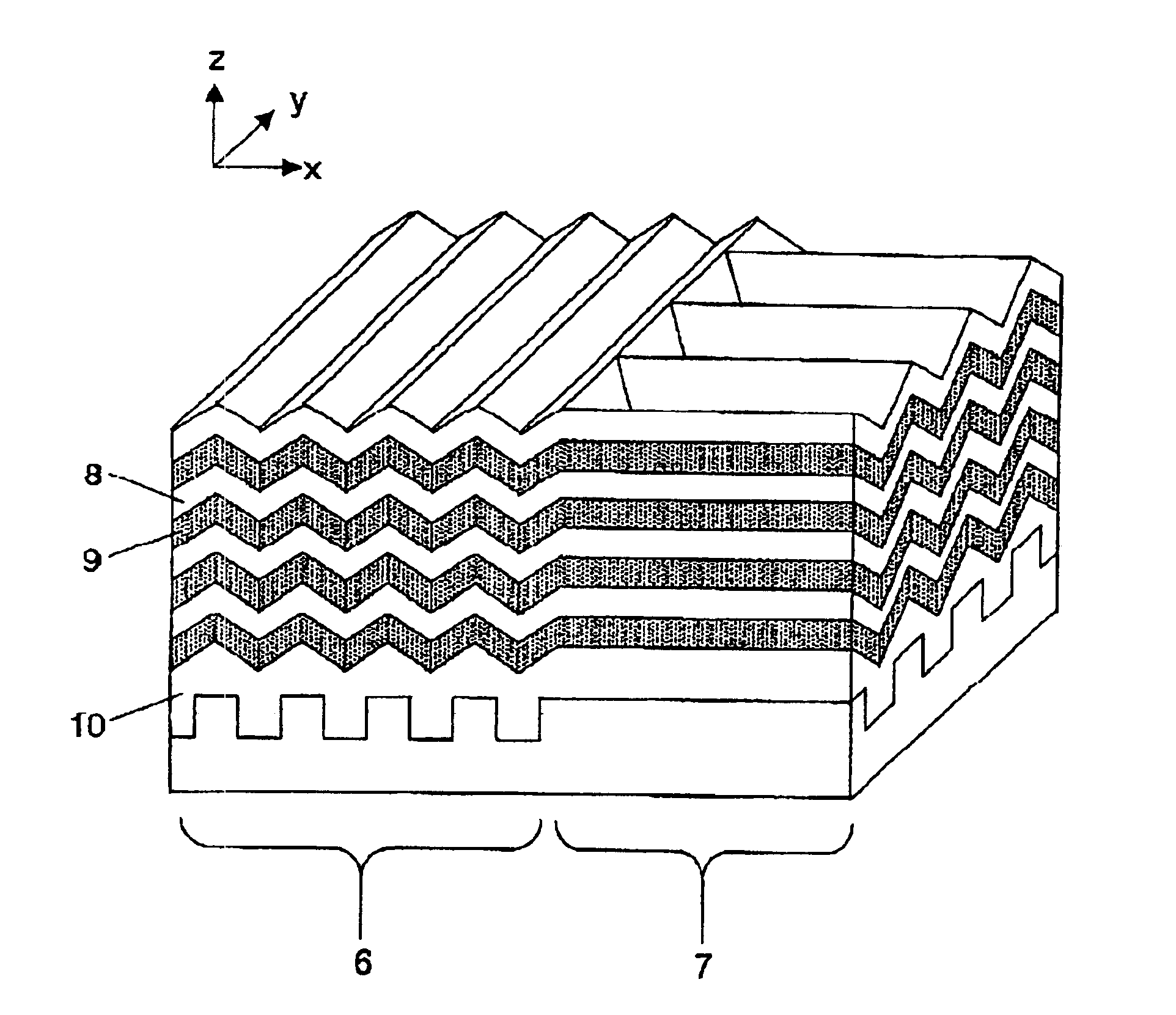
[0047]A polarizing element of the portion designated by symbol 3 in FIG. 3 is described. In the figure, symbol 8 is an amorphous SiO2 layer (SiO2 layer) and symbol 9 is an amorphous Si layer (Si layer). The period Lx in the x-axis direction is 0.5 μm and the period Lz in the z-axis direction is 0.57 μm. The SiO2 layer 8 and the Si layer 9 each have a zigzag shape along the x-axis direction. Symbol 7 shows a structure obtained by turning a structure of symbol 6 by 90 degrees.

[0048]Next, a method for making this structure is described.

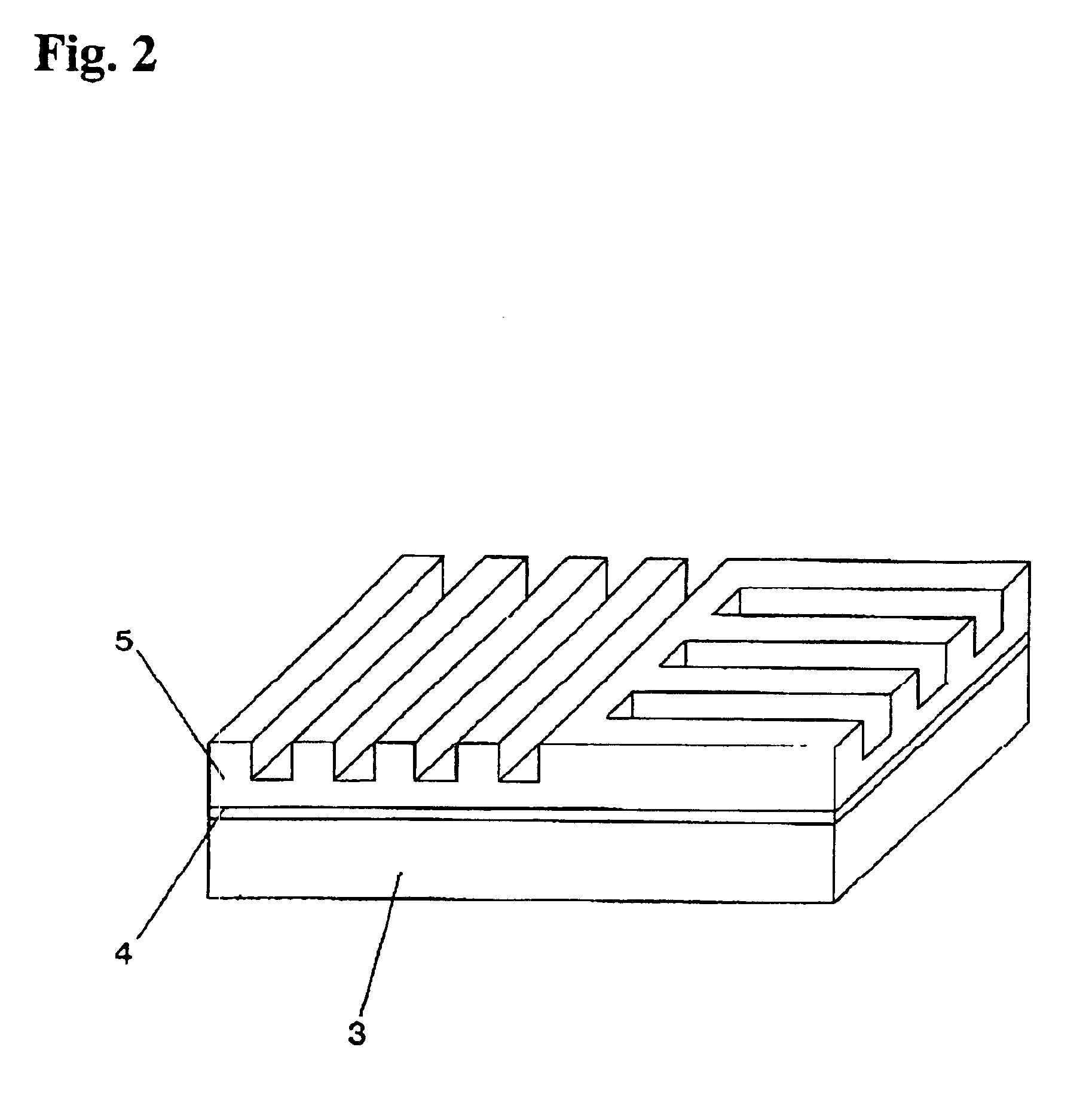
[0049]First, a periodical resist pattern is formed on a substrate by means of an electron beam lithography technique. The width of the groove is 0.25 μm, the depth is 0.2 μm and the period in the transverse direction is 0.57 μm. FIG. 2 shows a schematic figure of it. Symbol 3 is a substrate, symbol 4 is a reflection-free coating layer, and symbol 5 is a periodical groove portion. Generally, according to selection of the dimensions of a peri...

embodiment 2

(Embodiment 2)

[0060]In a similar structure to the portion of symbol 3 in FIG. 3, by properly determining the period of the pattern on a substrate and the period of deposition, it is possible to make the structure act as a wave plate providing an optional phase difference between polarized lights being perpendicular to each other. That is, a structure as shown in FIG. 3 provides an optical element with wave plates whose optical axes are directed in different directions according to locations, combined together. Further, since a structure with the same period of deposition can be made to act as a ½-wavelength plate or a ¼-wavelength plate by changing the period of the pattern of a substrate, it is possible to realize a ½-wavelength plate and a ¼-wavelength plate at the same time on a single substrate by making the period of the substrate different according to locations.

[0061]As application of such a device, there is an optical circulator (Japanese Patent Laid-Open Publication No.Hei ...

embodiment 3

(Embodiment 3)

[0063]Regions that are different by 90 degrees in direction of grooves from each other are alternately arranged two-dimensionally like a pattern shown in FIG. 6. In such a structure, assuming that the structures in symbol 13 and symbol 14 are similar to those of symbols 6 and 7, the portion of symbol 13 reflects a polarized light in the x direction and transmits a polarized light in the y direction. On the other hand, the portion of symbol 14 transmits a polarized light in the x direction and reflects a polarized light in the y direction. By making the region of symbol 13 and the region of symbol 14 equal in area to each other, any polarized light of an incident light in the z direction is reflected by one of regions of symbols 13 and 14 and is transmitted by the other. That is, an optical element can be produced in which 50% of incident power is reflected and the other 50% of it is transmitted regardless of the polarized state of the incident. This action is possible ...


PUM

PropertyMeasurementUnit
depthaaaaaaaaaa
depthaaaaaaaaaa
depthaaaaaaaaaa

Abstract

The optical element includes photonic crystals respectively having different optical characteristics. These photonic crystals are formed in a plurality of regions on a single substrate. The optical element has a structure in which two or more kinds of media are nearly periodically deposited on one-dimensionally periodical grooves. Further, the grooves are different in direction according to locations on the deposited surface. A variety of optical elements each having different dependencies on polarization according to locations can be obtained. That is, portions or zones different in optical characteristics can be integrated on a single substrate.

Description

BACKGROUND OF THE INVENTION[0001]1. Field of the Invention[0002]The present invention relates to an integrated optical element with a plurality of regions that differ in optical characteristic according to locations, wherein said regions each are of a structure with a two-dimensional or three-dimensional periodicity in refractive index and are combined together so that the periodicities in refractive index of said regions are different in direction from each other, and a method for making the same.[0003]2. Description of the Related Art[0004]Optical materials that have been used up to now are materials existing in the natural world, and they are classified into amorphous materials and crystalline materials. An amorphous material has no dependency on direction in optical characteristic. A crystalline material is anisotropic in relation between its crystal axes and the traveling direction or polarization direction of light. However, such a direction is specifically determined in a cry...

Claims


Application Information

Patent Timeline
Patent Type & Authority Patents(United States)
IPC IPC(8): G02F1/00G02B6/12G02B5/18G02B5/30G02B6/122G02B6/126G02B6/132
CPCB82Y20/00G02B6/1225G02B6/126G02B6/132
Inventor KAWAKAMI, SHOJIROKAWASHIMA, TAKAYUKIISHIKAWA, WATARUSATO, TAKASHI
Owner PHOTONIC LATTICE
Why Eureka
Try Eureka