Methods and apparatuses for assembling elements onto a substrate

a technology of substrate and assembly method, which is applied in the manufacture of cables/conductor parts, chemistry apparatus and processes, transistors, etc., can solve the problems of limited conductivity, difficult to produce a completely flawless active matrix liquid crystal display (lcd), and inability to completely flawlessly achieve the effect of active matrix and substrate friction reduction

Inactive Publication Date: 2006-11-28
RUIZHANG TECH LTD CO
View PDF6 Cites 91 Cited by
  • Summary
  • Abstract
  • Description
  • Claims
  • Application Information

AI Technical Summary

Benefits of technology

[0012]The present invention relates to methods and apparatuses for assembling elements onto a substrate. The surface of the elements and / or the substrate are treated and the elements are dispensed over the substrate in a slurry. Typically, the elements assembly onto receptor regions of the substrate in a process known as fluidic self assembly, and the receptor regions (e.g. holes in the substrate) are designed to receive the elements. The treatment of surfaces of the elements and / or surfaces of the substrate is usually designed to reduce the friction between the elements and the substrate as the elements slide along a surface of the substrate. The treatment of the surfaces usually, but not necessarily, alters both sets of surfaces so that they are of the same type. For example, both the elements and substrate may be treated to have a hydrophilic surface and the elements, so treated, may be dispersed in a polar solvent (e.g. H2O) and then dispensed over the so treated substrate in an FSA process. In an alternative example, both the elements and the substrate may be treated to have a hydrophobic surface and the elements and substrate, so treated, may be combined in a solvent (e.g. hexane) which is non-polar in an FSA process.

Problems solved by technology

As is well known in the art, it is difficult to produce a completely flawless active matrix liquid crystal display (LCD), when the display area is large, such as the LCD's on modern laptop computers.
Silicon VLSI can be used to produce such an array over a silicon wafer's surface, but silicon wafers are limited in size, limited in conductivity, and not transparent.
Further, processing of large areas on silicon wafers can be expensive.
Single crystal silicon can be bonded to a glass substrate and then etched to remove most of the area to achieve transparency, but this is intrinsically wasteful in that, for the sake of maximizing light transmission, the majority of the processed material is discarded and becomes chemical waste.
The under-utilization of the precious die area wastes resources, causes greater amounts of chemical waste to be generated in the process, and is generally inefficient and expensive.
Large arrays of silicon photodiodes with concentrating lenses have been made by sawing wafers and using a pick and place assembly, but thermal dissipation is poor for large elements, and the small elements require too much assembly time.
These approaches avoid the limitations of the size of the available single crystal silicon wafers, and avoid the cost of the single crystal wafers, but require expensive deposition of the semiconductor layer, and they still require processing of the entire large substrate to form the active elements in an array, still resulting in the production of much chemical waste and wasted resources.
These processes also limit the choice of the substrate; for example, plastic substrates cannot be used due to the nature of the processes which deposit the semiconductor layers.
Furthermore, amorphous or polycrystalline silicon semiconductor elements do not perform as well as those made from single crystal semiconductor material.
For displays, as an example, it is often difficult or impossible to form some of the desired circuitry out of the amorphous or polycrystalline semiconductor materials.
Thus, high frequency edge drivers may be impossible to form out of these materials.
This results in the difficulty and expense of attaching an electrical lead for each and every row and column of an array, such as an active matrix liquid crystal display array.
As noted above, another difficulty with the existing techniques is that the large number of elements in a large array results in a low probability that all of them will work properly and thus the yield of acceptably good arrays from the manufacturing process is low.
Furthermore, there is no possibility of testing any of the elements until the assembly is complete, and then any imperfection in the array must be tolerated or the entire array could be discarded or special and expensive techniques must be used to repair it.
These problems result from the fact that the various elements in the array are fabricated on the array rather than separately.
Pick and place methods place devices generally one at a time, and are generally not applicable to very small or numerous elements such as those needed for large arrays, such as an active matrix liquid crystal display.
The structure shown in FIG. 2D has the drawback that a monocrystalline silicon layer is required in order to use the KOH etch to form the hole.
Even if the opening is perfectly formed, the fluidic self assembly process can still produce poor results if the elements do not flow smoothly over the surface containing the openings.
If the elements remain stuck to the surface during planarization and interconnect metallization, the completion of an assembly with these stuck elements will potentially destroy metal electrical interconnects or other functional features.

Method used


Image

  • Methods and apparatuses for assembling elements onto a substrate
  • Methods and apparatuses for assembling elements onto a substrate
  • Methods and apparatuses for assembling elements onto a substrate

Examples


Embodiment Construction

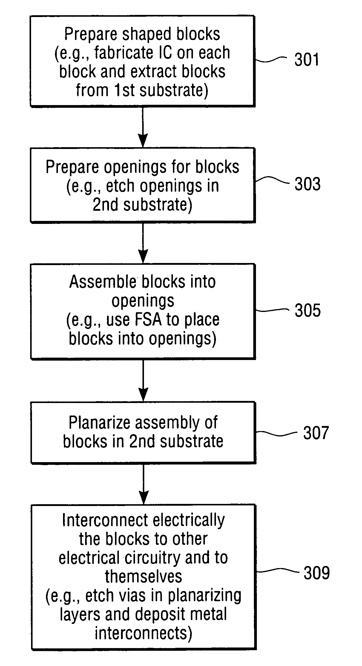
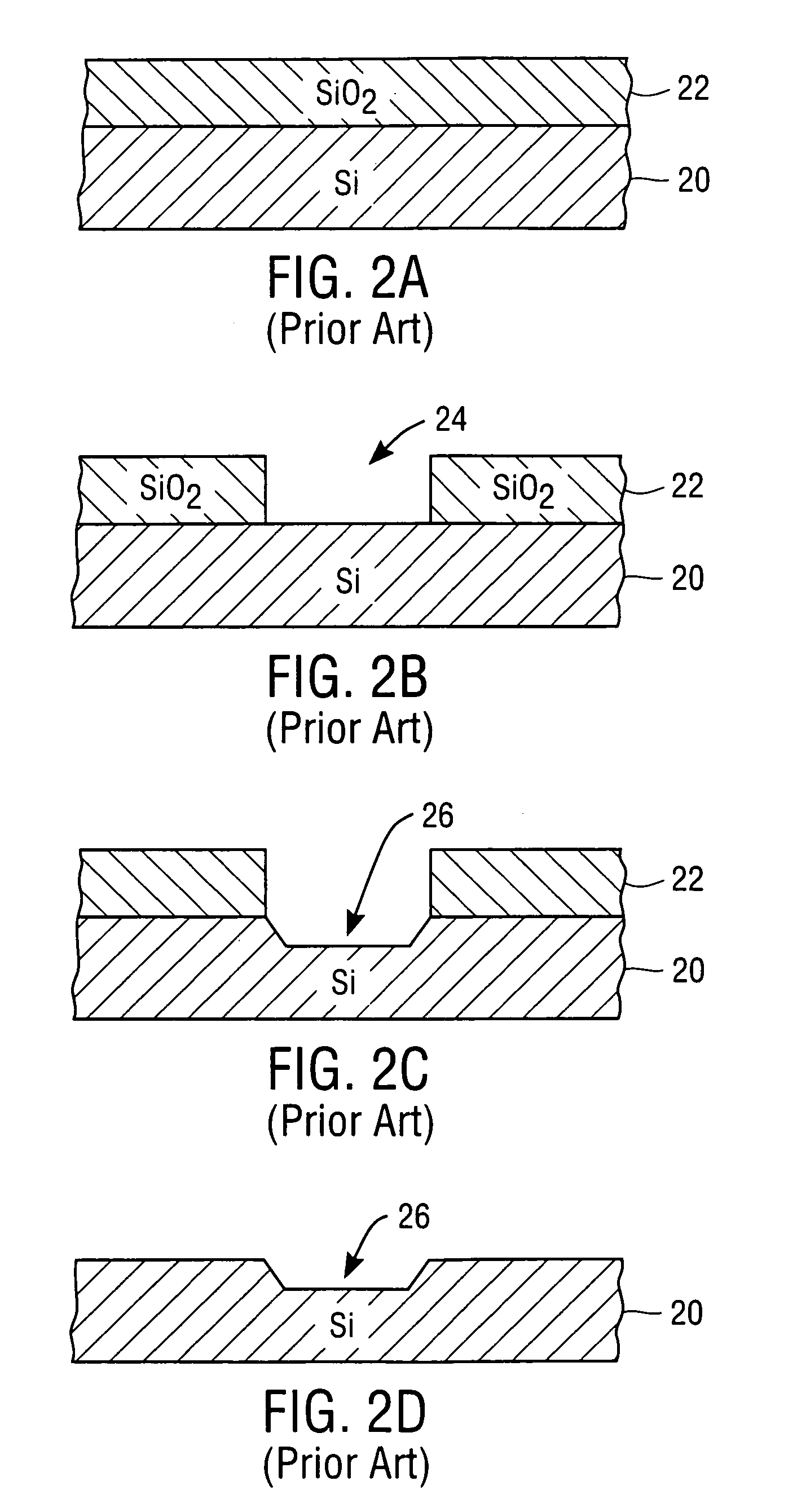
[0035]The present invention relates to methods and apparatuses for forming openings in a receiving substrate. The following description and drawings are illustrative of the invention and are not to be construed as limiting the invention. Numerous specific details are described to provide a thorough understanding of the present invention. However, in certain instances, well known or conventional details are not described in order to not unnecessarily obscure the present invention in detail.

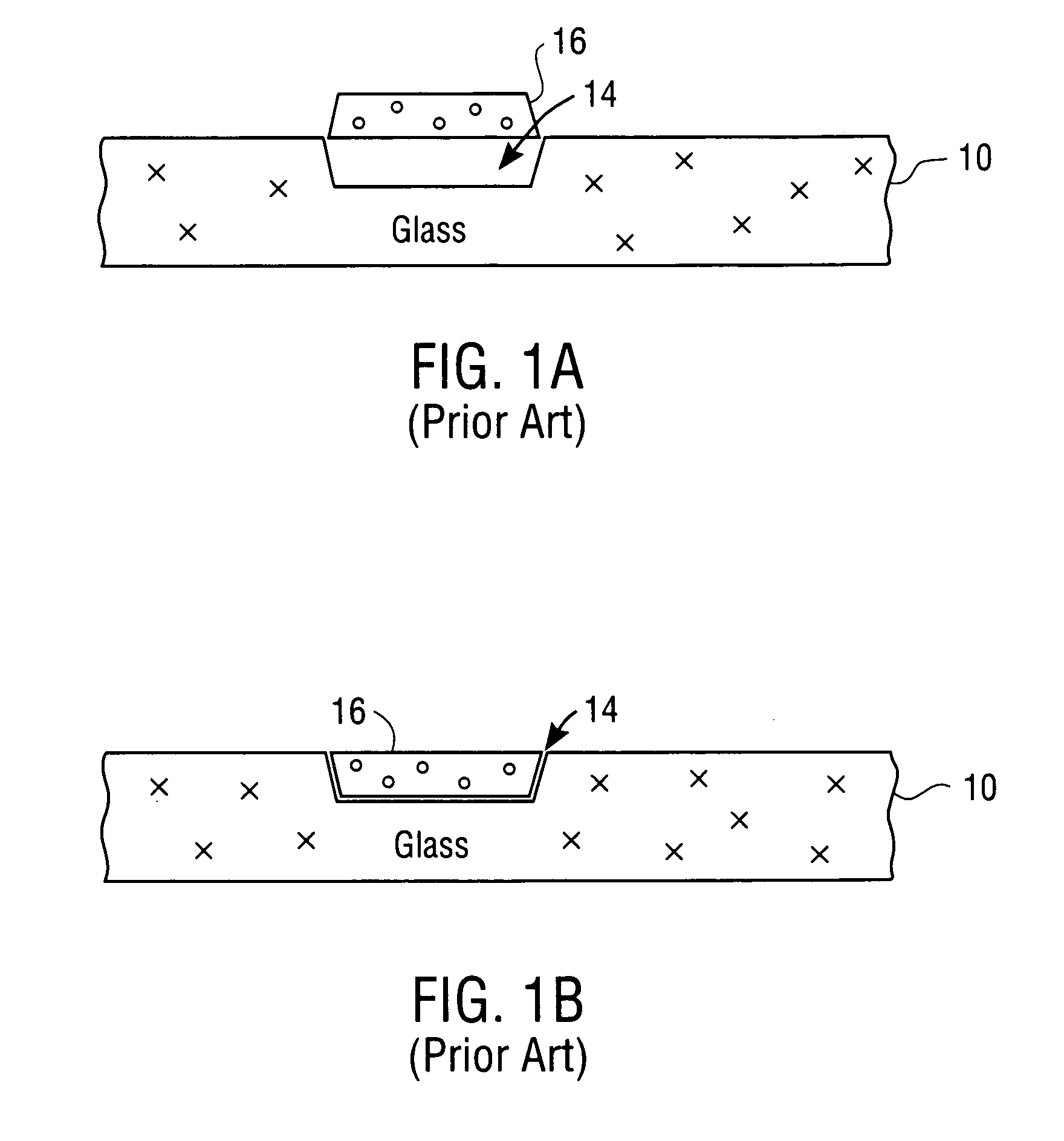
[0036]The present invention relates generally to the field of creating openings in a receiving substrate and to apparatuses having these openings. The present invention may be used to fabricate openings for various different types of arrays. Typically, each element in the array includes a functional component which may be an electrical component, a chemical component, or an electromechanical structural element or a micro electromechanical structural element or a micro-mechanical structural element....


PUM

PropertyMeasurementUnit
thicknessaaaaaaaaaa
thicknessaaaaaaaaaa
sizeaaaaaaaaaa

Abstract

Methods and apparatuses for assembling elements onto a substrate. The surfaces of the elements and/or the substrate are treated and the elements are dispensed over the substrate in a slurry. In one example of the invention, the substrate is exposed to a surface treatment fluid to create a surface on the substrate which has a selected one of a hydrophilic or a hydrophobic nature, and a slurry is dispensed over the substrate. The slurry includes a fluid and a plurality of elements (each of which includes a functional component). Each of the plurality of elements is designed to be received by a receptor region on the substrate. The dispensing of the slurry with the fluid occurs after the substrate is exposed to the surface treatment fluid, and the fluid is the selected one of a hydrophilic or a hydrophobic nature. In another example of the invention, a plurality of elements is exposed to a surface treatment fluid to create surfaces on the elements having a selected one of a hydrophilic or a hydrophobic nature. A slurry is dispensed over a substrate, wherein the slurry contains a fluid and the plurality of elements which are designed to be received by a plurality of receptor regions. The fluid is the selected one of a hydrophilic or hydrophobic nature. In another example of an aspect of the invention, a surfactant is used with a slurry having elements which are deposited onto receptor regions in a fluidic self assembly process. Other examples of methods are also described.

Description

RELATED APPLICATIONS[0001]This is a Continuation of U.S. patent application Ser. No. 09 / 432,289, filed on Nov. 2, 1999, U.S. Pat. No. 6,527,964.FIELD OF THE INVENTION[0002]The present invention relates generally to the field of fabricating openings in a substrate and also to apparatuses with these openings. More particularly, the present invention relates to methods for forming openings in a substrate which openings are designed to receive an element which is later placed into the opening and which element includes at least one functional component, and the present invention relates to methods for creating assemblies with the openings.BACKGROUND OF THE INVENTION[0003]There are many examples of large arrays of functional components which can provide, produce or detect electromagnetic signals or chemicals or other characteristics. An example of such a large array is that of a display where many pixels or sub-pixels are formed on an array of electronic elements. For example, an active ...

Claims


Application Information

Patent Timeline
Patent Type & Authority Patents(United States)
IPC IPC(8): H01L21/00B44C1/22H01L21/3065H01L21/336H01L21/60H01L21/77H01L21/98H01L29/786
CPCB82Y30/00H01L24/24H01L24/32H01L24/82H01L24/95H01L24/97H01L25/50H01L27/1214H01L29/66772H01L29/78603H01L29/78654H01L2224/24225H01L2224/24227H01L2224/73267H01L2224/95085H01L2224/95092H01L2224/95122H01L2224/97H01L2924/01005H01L2924/01011H01L2924/01013H01L2924/01027H01L2924/01047H01L2924/01074H01L2924/01082H01L2924/10158H01L2924/10253H01L2924/14H01L2924/15153H01L2924/15155H01L2924/15165H01L2924/15788H01L2224/82H01L2924/01006H01L2924/01019H01L2924/01033H01L2924/01072H01L2924/01084H01L2924/12041H01L2924/12043H01L2924/00
Inventor SMITH, JOHN STEPHENHADLEY, MARK A.CRAIG, GORDON S. W.NEALEY, PAUL F.
Owner RUIZHANG TECH LTD CO
Why Eureka
Try Eureka