Manufacturing method of silicon carbide single crystals
a manufacturing method and silicon carbide technology, applied in the direction of single crystal growth, polycrystalline material growth, thin material processing, etc., can solve the problems of internal stress at the crystal boundary, decrease in backward withstand voltage, leakage current of the device, etc., to facilitate growth at the opening, easy to occlude, and open the micro-pipe
- Summary
- Abstract
- Description
- Claims
- Application Information
AI Technical Summary
Benefits of technology
Problems solved by technology
Method used
Image
Examples
first embodiment
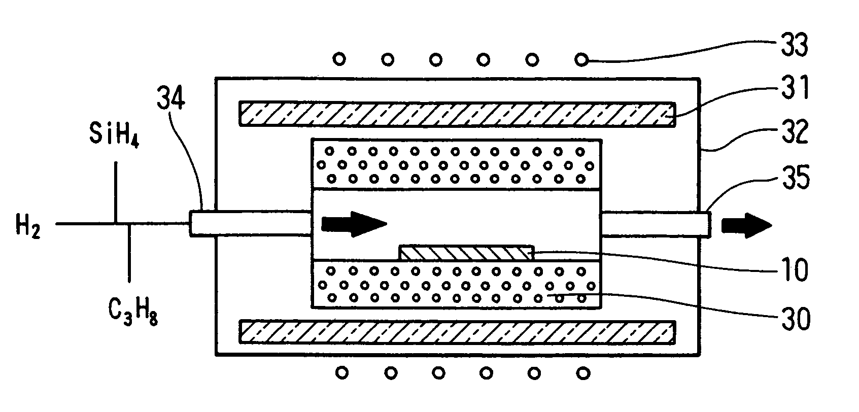
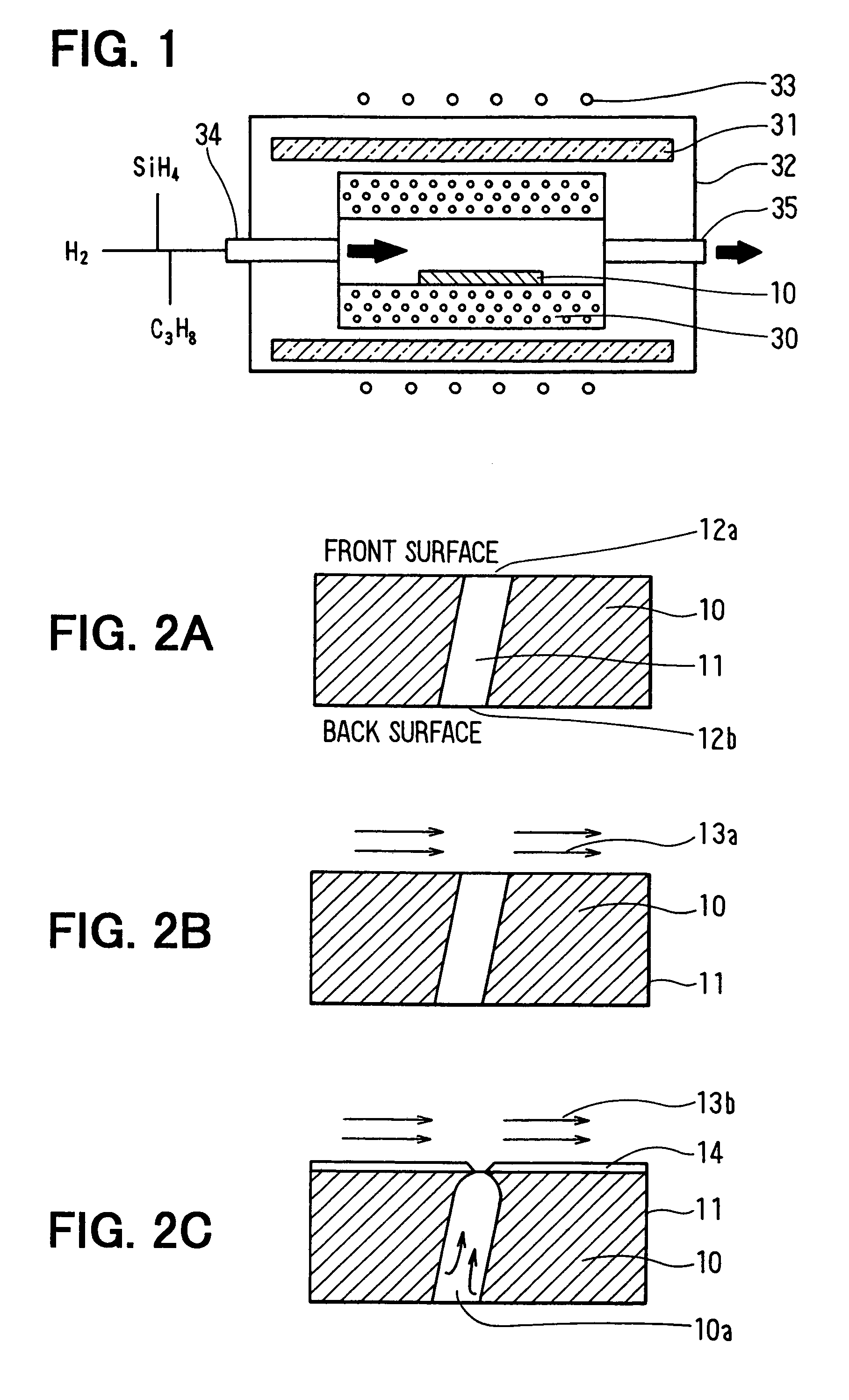
[0045]FIG. 1 is a schematic view of a CVD apparatus for growing a SiC epitaxial film in the first embodiment;
[0046]FIGS. 2A to 2C are cross sectional views showing epitaxial growth process in the first embodiment, respectively;
[0047]FIGS. 3A and 3B are cross sectional views showing epitaxial growth process in the first embodiment, respectively;
second embodiment
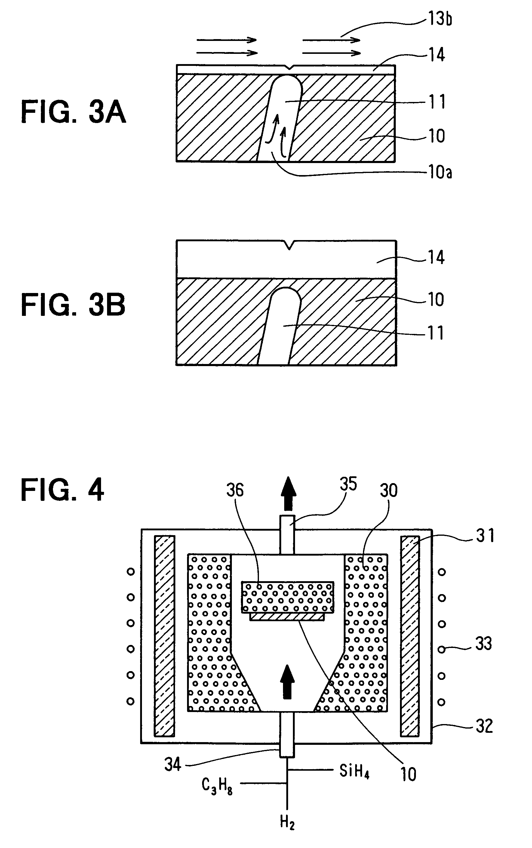
[0048]FIG. 4 is a schematic view of a CVD apparatus for growing a SiC epitaxial film in the second embodiment;
[0049]FIGS. 5A and 5B are cross sectional views showing epitaxial growth process in the second embodiment, respectively;
[0050]FIGS. 6A and 6B are cross sectional views showing epitaxial growth process in the second embodiment, respectively;
third embodiment
[0051]FIGS. 7A and 7B are cross sectional views showing epitaxial growth process in the third embodiment, respectively;
[0052]FIGS. 8A and 8B are cross sectional views showing epitaxial growth process in the third embodiment, respectively;
[0053]FIG. 9A is a cross sectional view of the SiC epitaxial growth substrate;
[0054]FIG. 9B is a cross sectional view of the SiC epitaxial growth substrate in the other embodiment, and
[0055]FIGS. 10A and 10B are cross sectional views showing modifications of the CVD apparatus in the second embodiment, respectively.
DETAILED DESCRIPTION OF THE PREFERRED EMBODIMENTS
[0056]Hereinafter, an embodiment adopting the present invention will be explained. The present embodiment adopts the present invention to a method for producing an epitaxial film for forming a device such as a field effect transistor (MOSFET or the like), a junction field effect transistor (JFET), or a Schottky barrier diode on a silicon carbide single crystal substrate (SiC single crystal s...
PUM
 Abstract
Description
Claims
Application Information


