Semiconductor storage device and refresh control method therefor

a technology of semiconductors and storage devices, applied in the field of semiconductor storage devices, can solve the problems of reducing the retention time to as low as 200 ms, affecting the efficiency of reducing standby current, so as to achieve the effect of preventing the increase of chip area, and facilitating the improvement of standby current efficiency

Inactive Publication Date: 2007-01-23
LONGITUDE SEMICON S A R L
View PDF7 Cites 45 Cited by
  • Summary
  • Abstract
  • Description
  • Claims
  • Application Information

AI Technical Summary

Benefits of technology

[0013](A) It is assumed that the refresh period for a 256 Mbit DRAM is sorted at an elevated temperature (for example, at T=85° C., in terms of 32 Kbits for a main word line, with a long period (such as 1 s) and with a short period (such as 100 ms). In this case, with 20000 bit memory cells, with the retention time not longer than 1 s, the main word line (MWL) in need of refresh with the short period (100 ms) is increased to e.g. one bank (64 Mbits). Hence, the efficacy of reducing the standby current is not larger than three fourths.
[0035]According to the present invention, the chip area may further be prevented from increasing by providing an error detection circuit of a simpler structure on a bit line between the memory cell array and the sense amplifier.

Problems solved by technology

Hence, the efficacy of reducing the standby current is not larger than three fourths.(B) If the refresh period is sorted with the wafer test (test on a wafer prober), sorting failure occurs if retention time variations occur in a process following the package assembling.(C) In addition, at an elevated temperature of T=85° C., it may be an occurrence that the retention time is decreased to as low as 200 ms.
However, if the refresh is carried out frequently, the efficacy in reducing the standby current may not be improved.
The result is the increased current consumption in case the user repeats entry and exiting.(B) For the period for error correction (such as step S705 of FIG. 23), it is necessary to set the time duration for prohibiting a command from outside from being accepted.

Method used


Image

  • Semiconductor storage device and refresh control method therefor
  • Semiconductor storage device and refresh control method therefor
  • Semiconductor storage device and refresh control method therefor

Examples


first embodiment

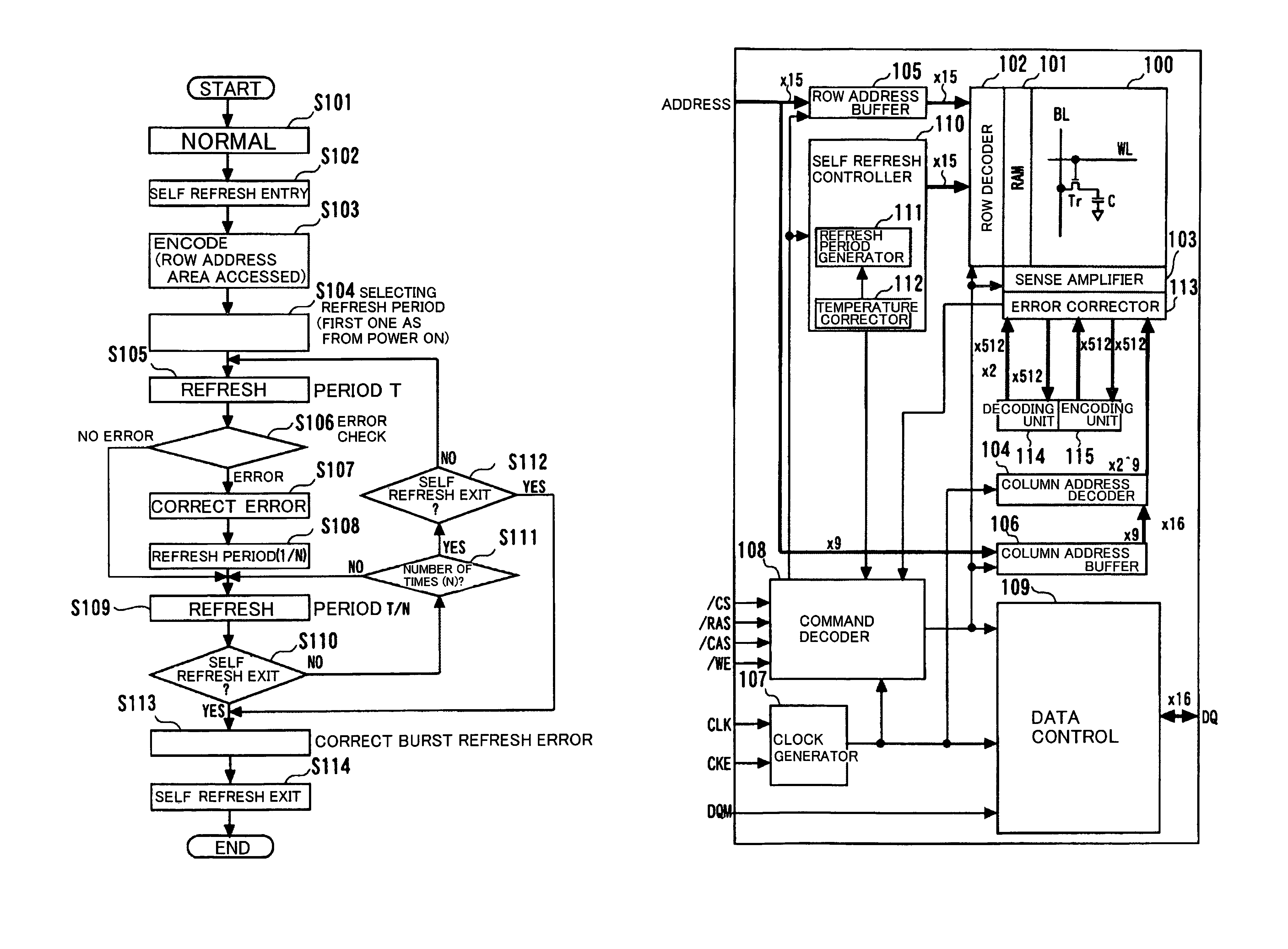
[0043]FIG. 1 is a flowchart for illustrating the operation of a semiconductor storage device according to the present invention.

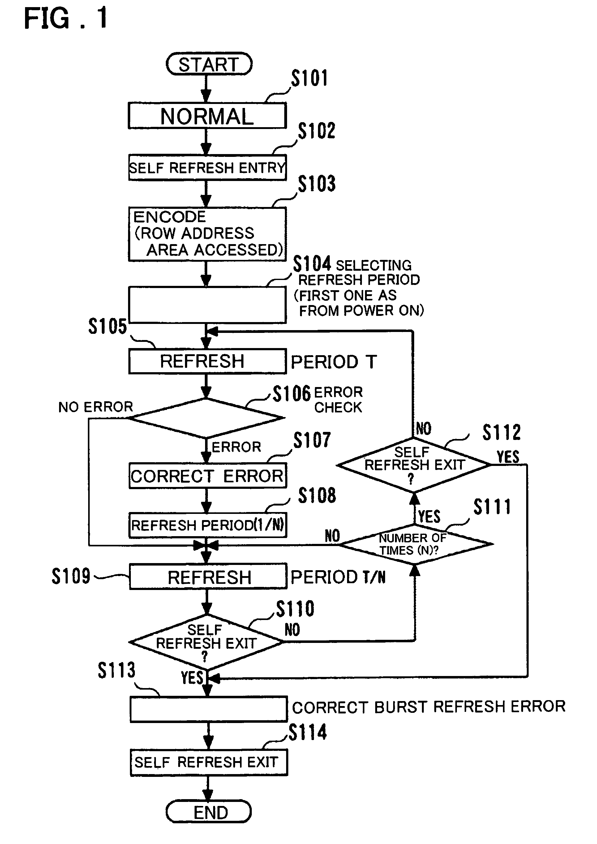
[0044]FIG. 2 is a diagram showing the configuration of the semiconductor storage device according to the first embodiment of the present invention.

[0045]FIG. 3 illustrates the recording of a row address in a RAM according to the first embodiment of the present invention.

[0046]FIG. 4 illustrates the encoding in the first embodiment of the present invention.

[0047]FIG. 5 illustrates readout of the refresh information in the first embodiment of the present invention.

[0048]FIG. 6 illustrates error detection and error correction in the first embodiment of the present invention.

[0049]FIG. 7 is a diagram showing the configuration of a one bit error detector in the first embodiment of the present invention.

[0050]FIG. 8 is a flowchart for illustrating the selecting of a refresh period in the first embodiment of the present invention.

[0051]FIGS. 9A,9B and 9C illustrat...

second embodiment

[0055]FIG. 13 is a flowchart for illustrating the processing of a four-value adaptive refresh period according to the present invention.

[0056]FIG. 14 is a flowchart for illustrating the selecting processing of the four-value adaptive refresh period according to a second embodiment of the present invention.

[0057]FIG. 15 illustrates the selecting processing of the four-value adaptive refresh period according to a second embodiment of the present invention.

[0058]FIG. 16 illustrates the relationship between the current consumption and the transition of the inner state in the second embodiment of the present invention (first one after power up).

[0059]FIG. 17 illustrates the relationship between the current consumption and the transition of the inner state in the second embodiment of the present invention (second one after power up).

[0060]FIG. 18 illustrates the four-value adaptive refresh of the second embodiment of the present invention and a Comparative Example.

third embodiment

[0061]FIG. 19 shows the overall configuration of the present invention.

[0062]FIG. 20 is a flowchart for illustrating the operation of an embodiment of the present invention.

[0063]FIGS. 21A and 21B illustrate the relationship between the current consumption and the transition of the inner state in the second embodiment of the present invention (second and following ones one after power up).

[0064]FIG. 22 is a flowchart for illustrating an example of the conventional refresh control.

[0065]FIG. 23 is a flowchart for illustrating another example of the conventional refresh control.


PUM


Abstract

A dynamic semiconductor storage device in which the power supply current during the standby time is diminished to decrease the power consumption and to suppress the chip area from increasing. During the normal operation, the information as to a word line associated with a row address accessed during the normal operation is stored in a RAM. In entering self refresh, data of memory cells connected to a word line associated with a row address accessed during the normal operation time is read out and check bits for the data are appended in an encoder and written in a check bit area. As an initializing operation for the first self refresh entry after power up sequence, the data retention time of the memory cells is inspected every word line. Based on the results of inspection, the setting value of the refresh period of the word line is determined and written in the RAM to set the word line based refresh period. During error check for the refresh operation, any error is corrected by an error correction circuit.

Description

FIELD OF THE INVENTION[0001]This invention relates to a semiconductor storage device and, more particularly, to a dynamic semiconductor storage device having memory cells that are in need of refreshing for data retention, and a refreshing controlling method therefor.BACKGROUND OF THE INVENTION[0002]For reducing current consumption in a dynamic random access memory (DRAM) during the standby time when only data retention is made, it is indispensable to reduce the current during the refresh operation (the operation of amplifying data read out to a bit line from memory cells connected to the word line associated with the refresh address, and of re-storing the read-out data via the bit line).[0003]In the DRAM, where the storage capacity is becoming larger and larger and the miniaturization is advancing, attempts are being made to improve the worst case value of the data retention time of the memory cell by the fabrication process. By way of circuit designing countermeasures, such a techn...

Claims


Application Information

Patent Timeline
Patent Type & Authority Patents(United States)
IPC IPC(8): G11C7/00G06F11/10G11C7/10G11C11/401G11C11/403G11C11/406
CPCG06F11/1004G11C7/02G11C7/1006G11C7/20G11C11/406G11C11/40615G11C11/4072G11C11/4096G11C11/40626G11C2211/4067G11C2207/104G11C2211/4061G11C2211/4062
Inventor RIHO, YOSHIROITO, YUTAKA
Owner LONGITUDE SEMICON S A R L
Why Eureka
Try Eureka