Capacitor, circuit board with built-in capacitor and method of manufacturing the same

a technology of built-in capacitors and capacitors, which is applied in the direction of printed capacitor incorporation, printed capacitor incorporation, printed electric component incorporation, etc., can solve the problems of difficult formation of electrolytic polymerization films directly on the surface of dielectric layers, and affecting the effect of dielectric layer damag

Inactive Publication Date: 2007-01-30
SHINKO ELECTRIC IND CO LTD
View PDF8 Cites 5 Cited by
  • Summary
  • Abstract
  • Description
  • Claims
  • Application Information

AI Technical Summary

Benefits of technology

[0013]It is preferable that the conductive adhesive agent should be a paste-like adhesive agent containing a conductive organic material. Such a conductive adhesive agent enters an inside even if concavo-convex portions are provided on the surface of the first solid electrolytic layer or the second solid electrolytic layer. Consequently, it is possible to produce an advantage that the equivalent series resistance of the capacitor can be reduced and the bonding can be carried out firmly.
[0015]In the invention, it is preferable that both the first solid electrolytic layer and the second solid electrolytic layer should be formed by organic solid electrolytic layers. If they are formed by the organic solid electrolytic layers, it is possible to suppress or prevent the damage of the dielectric layer in a forming process thereof differently from the case in which manganese dioxide is sintered from a manganese nitrate solution.

Problems solved by technology

In a capacitor having such a structure, there is a problem of withstand voltage or leakage current, which is largely influenced by a solid electrolytic layer.
In this regard, in the case of forming an inorganic solid electrolyte such as manganese dioxide, the sintering step needs to be repetitively carry out for many times. When the sintering step is repeated, however, a dielectric layer might be damaged through the process.
For preventing this problem, the dielectric layer is necessarily formed with relatively thick, however, this causes another problem.
However, it is difficult to form the electrolytic polymerization film directly on the surface of the dielectric layer.
In this aspect, it causes further problem in that the property of the electrolytic polymerization film is apt to be varied by the influence of the unevenness.
Therefore, in the case in which a capacitor is fabricated in a wiring board to constitute a circuit board with built-in capacitor, if the thickness of the chemical polymerization film has such a large unevenness, it would make unevenness in the thickness of the circuit board with built-in capacitor, which would result in a fatal problem.

Method used


Image

  • Capacitor, circuit board with built-in capacitor and method of manufacturing the same
  • Capacitor, circuit board with built-in capacitor and method of manufacturing the same
  • Capacitor, circuit board with built-in capacitor and method of manufacturing the same

Examples


first embodiment

[First Embodiment]

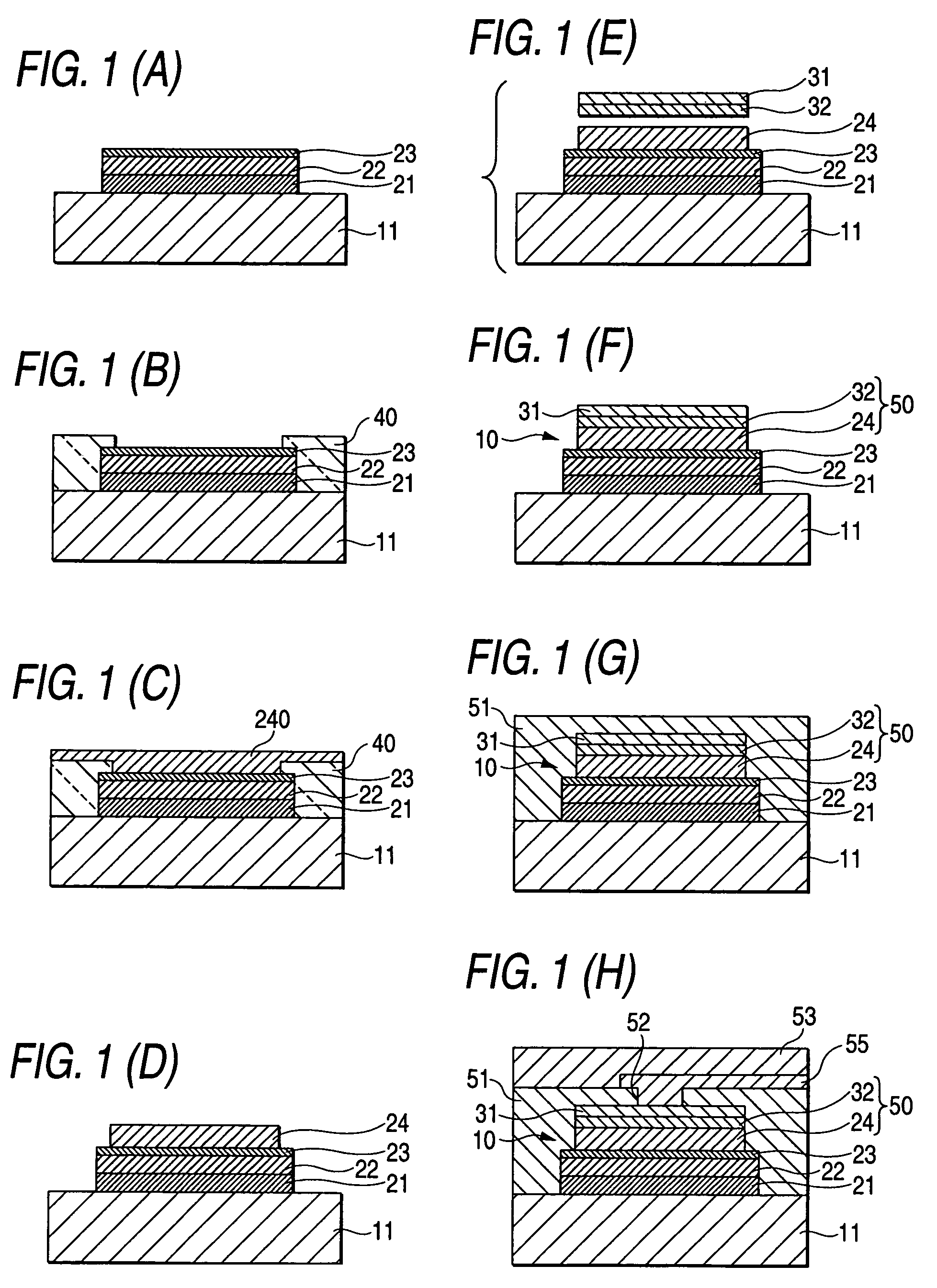
[0025]The structures of a capacitor and a circuit board with built-in capacitor according to a first embodiment of the invention will be described in detail with an explanation of methods of manufacturing them.

[0026]FIG. 1 is a sectional view showing steps in methods of manufacturing a capacitor and a circuit board with built-in capacitor to which the invention is applied. In the method of manufacturing a capacitor according to the embodiment, as shown in FIG. 1(A), a valve metal film 22 such as aluminum, tantalum, niobium, tungsten, vanadium, bismuth, titanium, zirconium, hafnium, their alloy or their compound (for example, niobium doped with oxygen) is formed on the surface of a first electrode 21 formed on a base material 11, and an anodic oxidation is then carried out to form a dielectric film 23 constituted by an anodic oxide film. In the embodiment, a tantalum film or a niobium film doped with oxygen is used as the valve metal film 22.

[0027]The base material ...

second embodiment

[Second Embodiment]

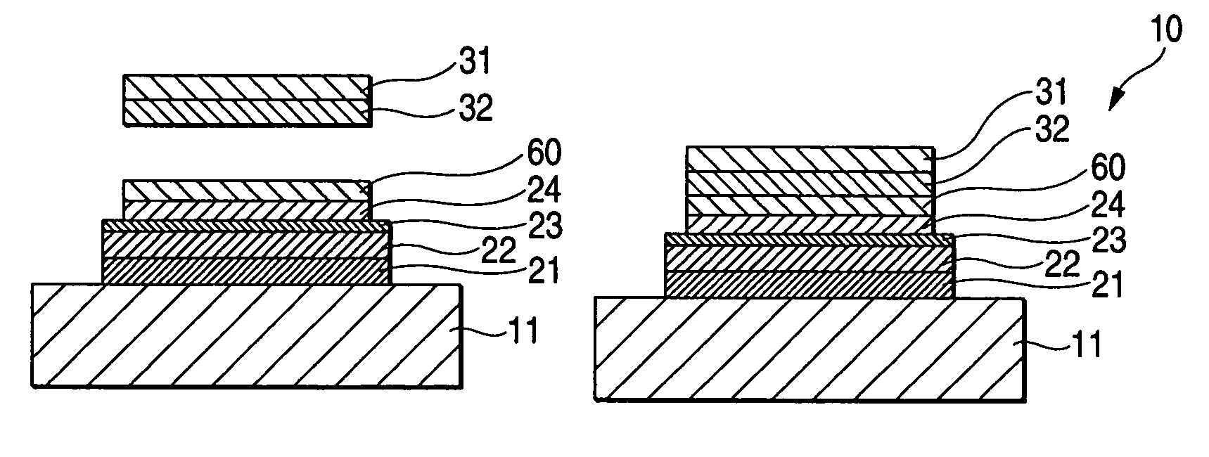
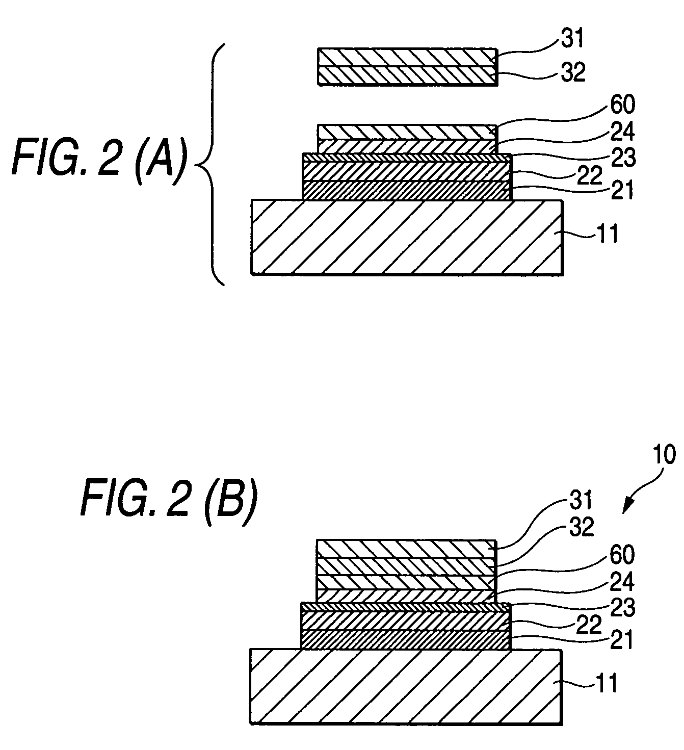
[0036]FIG. 2 is a sectional view showing steps in a method of manufacturing a capacitor according to a second embodiment of the invention.

[0037]In the embodiment, as shown in FIG. 2(A), a conductive adhesive agent 60 is provided between the surface of a first solid electrolytic layer 24 formed on a first electrode 21 and the surface of a second solid electrolytic layer 32 formed on a second electrode 31, where a heat press is carried out in this state so that bonding the first solid electrolytic layer 24 to the second solid electrolytic layer 32 can be made. By such a structure, the first solid electrolytic layer 24 and the second solid electrolytic layer 32 can be bonded firmly irrespective of the property of the solid electrolytic layer.

[0038]It is preferable that the conductive adhesive agent 60 should be a paste-like adhesive agent containing, as a conductive organic material, a conductive polymer such as polypyrrole or an organic semiconductor such as a TCNQ ...

third embodiment

[Third Embodiment]

[0039]FIG. 3 is a sectional view showing steps in a method of manufacturing a capacitor according to a third embodiment of the invention.

[0040]While the polar capacitor has been manufactured in the first and second embodiments, it is also possible to manufacture a non-polar (non-polar type) capacitor 10 by forming a valve metal film 33 on the surface of a second electrode 31 and then carrying out an anodic oxidation to form a dielectric layer 34 constituted by an anodic oxide film, and thereafter, forming a second solid electrolytic layer 32 on the surface of the dielectric layer 34 as shown in FIG. 3(A), and subsequently, bonding the surface of a first solid electrolytic layer 24, which is formed on a first electrode 21, to the surface of the second solid electrolytic layer 32, which is formed on the second electrode 31, with a paste-like conductive adhesive agent 60 interposed in-between. As a conductive organic material, a conductive polymer such as polypyrrole ...


PUM

PropertyMeasurementUnit
conductiveaaaaaaaaaa
dielectricaaaaaaaaaa
voltageaaaaaaaaaa

Abstract

In a capacitor 10, a first electrode 21, a dielectric layer 23, a solid electrolytic layer 50 and a second electrode 31 are provided. In a manufacturing process, the dielectric layer 23 and a first solid electrolytic layer 24 formed by a chemical polymerization film are provided on the first electrode 21 side, while a second solid electrolytic layer 32 formed by an electrolytic polymerization film is provided on the second electrode 31 side. Then, the solid electrolytic layers are bonded to each other.

Description

[0001]This application claims foreign priority based on Japanese Patent application No. 2004-4232, filed on Jan. 9, 2004, the contents of which is incorporated herein by reference in its entirety.BACKGROUND OF THE INVENTION[0002]1. Field of the Invention[0003]The present invention relates to a capacitor using a solid electrolyte, a circuit board with built-in capacitor, and methods of manufacturing the capacitor and the circuit board with built-in capacitor.[0004]2. Description of the Related Art[0005]A capacitor using a solid electrolyte has a structure in which at least a first electrode, a dielectric layer, a solid electrolytic layer and a second electrode are provided in this order. In conventional way for manufacturing such a capacitor, the dielectric layer is formed on the surface of an anode, which turns out to be the first electrode, by using a method such as an anodic oxidation and the solid electrolytic layer is then formed. Thereafter, a carbon paste or a silver paste is ...

Claims


Application Information

Patent Timeline
Patent Type & Authority Patents(United States)
IPC IPC(8): H01G9/00H01G9/028H01G9/02H05K1/16H05K3/46
CPCH01G9/028H05K1/162Y10T29/417H05K2201/09509H05K3/4602
Inventor SAKAGUCHI, HIDEAKIHIGASHI, MITSUTOSHIMOCHIZUKI, TAKASHI
Owner SHINKO ELECTRIC IND CO LTD
Why Eureka
Try Eureka