Flat panel display and fabrication method thereof

a technology of flat panel display and fabrication method, which is applied in the direction of optics, instruments, radio frequency control devices, etc., can solve the problem that the to-be-formed pixel electrode cannot achieve a higher pixel aperture ratio from behind

Active Publication Date: 2007-01-30
AU OPTRONICS CORP
View PDF8 Cites 15 Cited by
  • Summary
  • Abstract
  • Description
  • Claims
  • Application Information

AI Technical Summary

Benefits of technology

[0008]It is another object of the present invention to provide a method of forming a flat panel display with shorter distance between the edges of the second metal layer and the n+ doped silicon layer.

Problems solved by technology

Therefore, the to-be-formed pixel electrode cannot achieve a higher pixel aperture ratio from behind the edge of the metal layer (M2) because of parasitic capacitance between the pixel electrode and the n+ doped silicon layer.

Method used


Image

  • Flat panel display and fabrication method thereof
  • Flat panel display and fabrication method thereof
  • Flat panel display and fabrication method thereof

Examples


Embodiment Construction

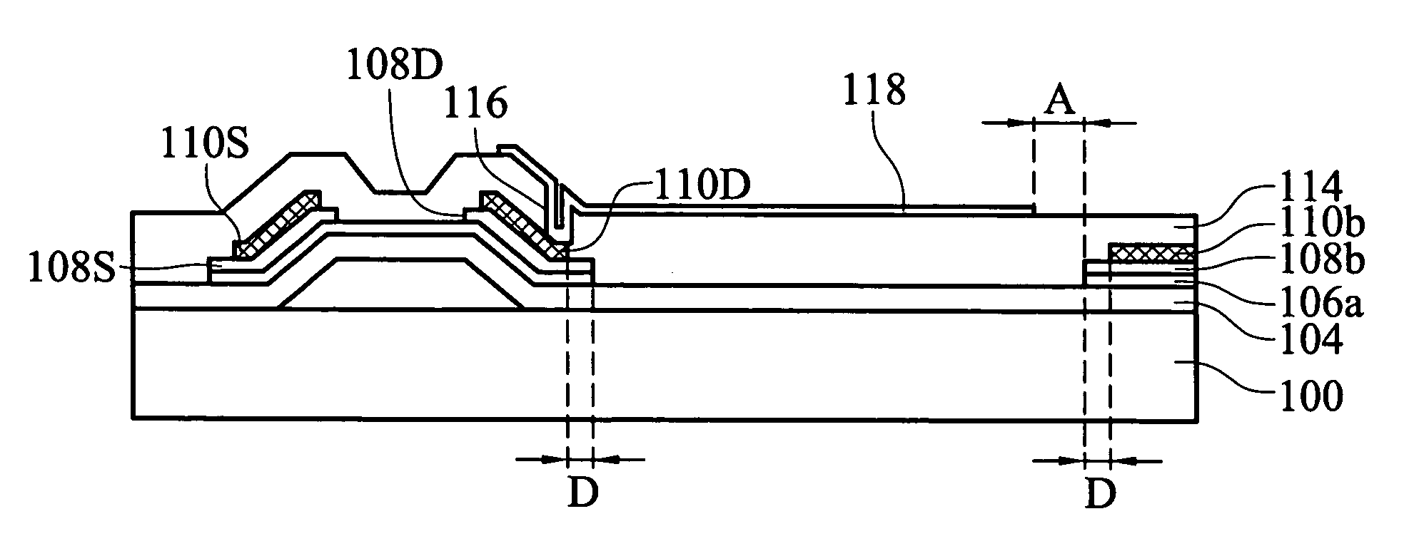
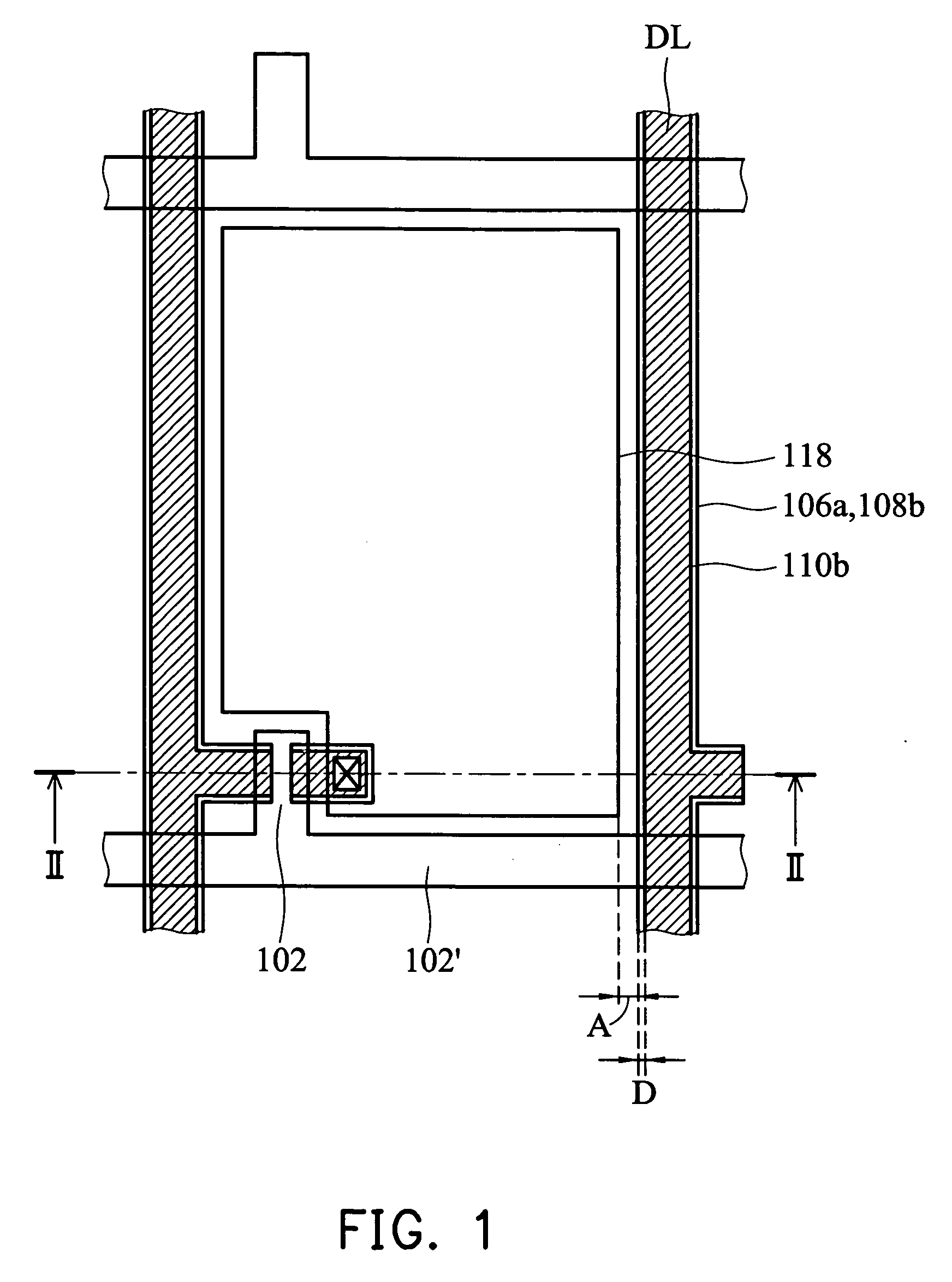
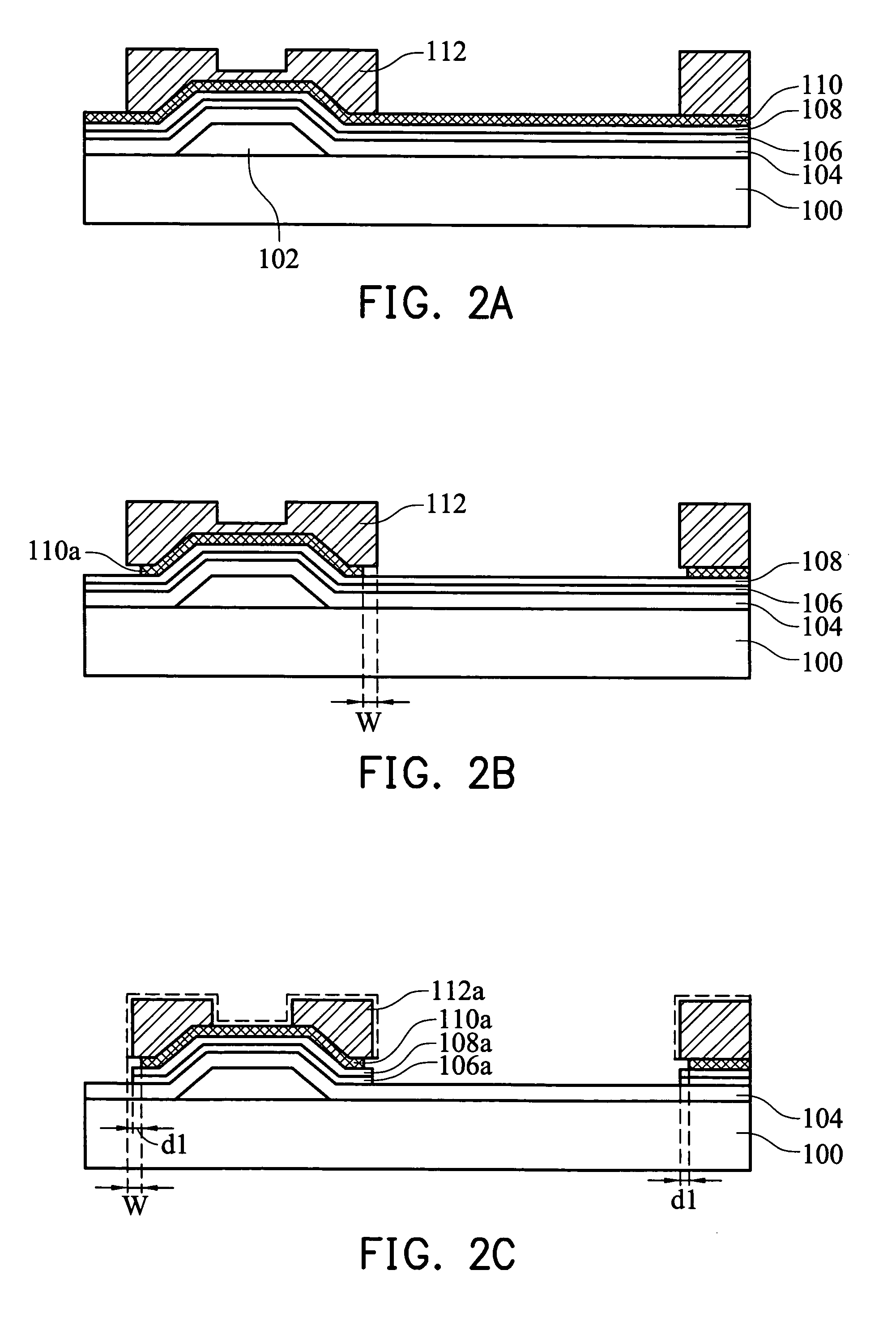
[0016]FIG. 1 is a top view of a flat panel display of the present invention. FIG. 2A˜2E are cross sections showing a method for forming the flat panel display, wherein FIG. 2E is a cross section of II—II cut line in FIG. 1.

[0017]Referring to FIG. 2A, a substrate 100, such as a glass or quartz substrate, is provided. A first conducting layer, such as a metal layer, is formed on the substrate 100, and patterned to form a gate electrode 102 and a gate line 102′, as shown in FIG. 1.

[0018]An insulating layer 104, a semiconductor layer 106, a doped semiconductor layer 108 and a second conducting layer 110 are sequentially formed on the substrate 100 with the gate line 102′ and the gate electrode 102 thereon. A resist layer 112 with double patterns is formed on the second conducting layer 110. The insulating layer 104 can be a silicon nitride layer or a silicon oxide layer. The semiconductor layer 106 can be an amorphous layer. The doped semiconductor layer 108 can be an n type doped amorp...


PUM


Abstract

A flat panel display and fabrication method thereof. The present invention uses four etching processes to define a second conducting layer, a doped semiconductor layer and a semiconductor layer. The first etching process is a wet etching using a first resist layer to etch the second conducting layer. The second etching process is executed with an etchant comprising oxygen to etch the doped semiconductor layer and the semiconductor layer, and the first resist layer undergoes ashing during etching so as to become a second resist layer with a channel pattern. The third etching process is another wet etching, and the second conducting layer is etched again using the second resist layer as the etching mask. The fourth etching process is executed to dry etch the doped semiconductor layer using the second resist layer as the etching mask.

Description

BACKGROUND OF THE INVENTION[0001]1. Field of the Invention[0002]The present invention relates in general to a flat panel display (FPD) and a fabrication method thereof. In particular, the present invention relates to a flat panel display with reduced parasitic capacitance and its fabrication method.[0003]2. Description of the Related Art[0004]Liquid crystal display (LCD) devices are a well-known form of flat panel displays with the advantages of low power consumption, light weight, thin profile, and low driving voltage. The liquid crystal molecules change orientation when an electronic field is applied. In the display region of the LCD, an array of pixel regions is patterned by horizontally extending gate lines and vertically extending data lines. Each pixel region has a thin film transistor (TFT) and a pixel electrode. The TFT serves as a switching device.[0005]The traditional TFT array substrate is fabricated by the following method. A gate insulating layer, an amorphous silicon l...

Claims


Application Information

Patent Timeline
Patent Type & Authority Patents(United States)
IPC IPC(8): H01L29/786H01L21/336H01L21/77H01L27/12H01L27/146
CPCH01L27/1214H01L27/1288H01L29/78618H01L29/66765H01L27/146
Inventor LAI, HAN-CHUNGLIAO, TA-WEN
Owner AU OPTRONICS CORP
Why Eureka
Try Eureka