Semi-insulating GaN and method of making the same

a semi-insulating gan and gan technology, applied in the direction of coatings, solid-state devices, chemical vapor deposition coatings, etc., can solve the problems of difficult device fabrication with small feature sizes, difficult to use foreign substrates, and yield a commercially viable large-area single-crystal semi-insulating gallium nitride material

Inactive Publication Date: 2007-01-30
WOLFSPEED INC
View PDF22 Cites 108 Cited by
  • Summary
  • Abstract
  • Description
  • Claims
  • Application Information

AI Technical Summary

Benefits of technology

[0015]FIG. 1 is a graph of resistivity as a function of inverse temperature for an iron-doped GaN crystal grown in accordance with Example 2 hereof.

Problems solved by technology

However, due to a lack of large area native GaN substrates, most GaN devices have been grown on non-native (heteroepitaxial) substrates such as sapphire and silicon carbide.
The use of such foreign substrates is problematic due to lattice mismatch and TE (thermal expansion) mismatch between GaN and the substrate material.
One consequence of TE mismatch is bowing of the GaN / heteroepitaxial substrate structure, which leads in turn to cracking and difficulty in fabricating devices with small feature sizes.
All of these approaches are susceptible to TE mismatch issues, and the resultant bowing, cracking and small feature fabrication difficulties discussed above, and none of such approaches has yielded a commercially viable large-area single-crystal semi-insulating gallium nitride material.

Method used


Image

  • Semi-insulating GaN and method of making the same
  • Semi-insulating GaN and method of making the same
  • Semi-insulating GaN and method of making the same

Examples


example 1

HVPE GaN Growth Incorporating Multiple Transition Metal Elements

[0087]In this example, the efficiency of incorporating transition metals in GaN crystals was determined in an HVPE process.

[0088]One weight percent of each of Cu, Ni, Co, Fe, Mn, and Cr, was added together with the others of such metals, in the gallium boat of an HVPE GaN growth system. After the HVPE reactor was heated to the growth conditions, gallium nitride crystals were grown under the same growth conditions as used for HVPE growth of gallium nitride without transition metal impurities.

[0089]The growth conditions were: growth temperature=1030° C., growth pressure=50 Torr, and growth rate=˜100 μm / hour. The transition metal impurity concentration in the grown GaN crystal was analyzed using glow discharge mass spectrometry (GDMS) by a commercial vendor.

[0090]Table I below shows the concentration of impurities in a GaN crystal grown in this example. The concentration of each of Cr, Mn and Co was below the detection lim...

example 2

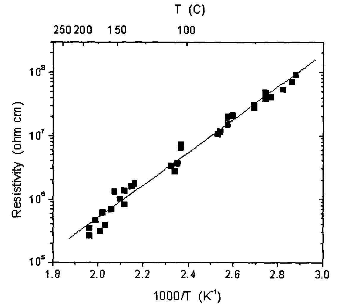
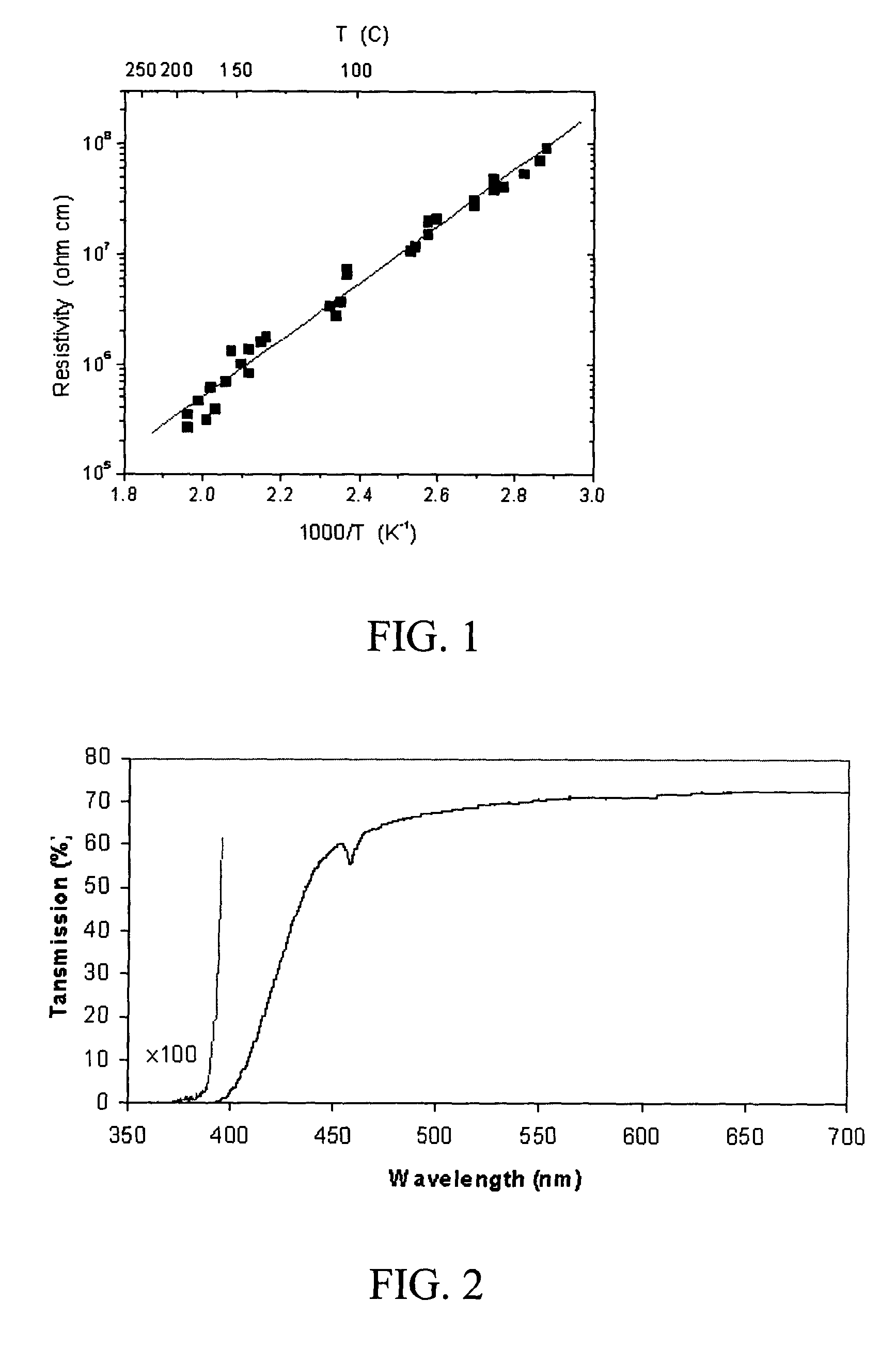
Semi-Insulating HVPE GaN Using Low-level Iron Doping

[0092]In this example, the growth and properties of semi-insulating HVPE GaN crystals were demonstrated by incorporating low concentration iron impurity. 2.8 grams of 99.995% pure iron and 250 grams of 99.99999% gallium were loaded into the gallium boat (reservoir) at room temperature. The reactor was sealed and the reactor temperature was raised to the growth temperature.

[0093]GaN crystals were grown on a sapphire template using the baseline growth conditions. The growth conditions were: growth temperature=1030° C., growth pressure=50 Torr, and growth rate=about 100 μm / hour. After four-hour growth, the GaN crystals were removed from the reactor and characterized.

[0094]Table II below shows the impurity concentration in a GaN crystal grown in this example. The impurity concentration was measured with secondary ion mass spectrometry (SIMS) by commercial vendor. The iron concentration was about 4×10¹⁶ Fe atoms cm-3, which was slightly...

example 3

Conductive HVPE GaN Using Low-level Iron Doping but with High Donor Impurities

[0097]In this example, the importance of reducing the background donor impurity concentration was demonstrated. This example used a different HVPE reactor configuration than the reactor that was used in Example 2.

[0098]5 grams of 99.995% pure iron and 800 grams of 99.99999% gallium were loaded into the gallium boat (reservoir) at room temperature (˜25° C.). The reactor was sealed and the reactor temperature was raised to the growth temperature. GaN crystals were grown on a sapphire template using the baseline growth conditions. The growth conditions were: growth temperature=1030° C., growth pressure=400 Torr, and growth rate=about 200 μm / hour. Sacrificial growth was carried out prior to the steady state growth process, to let the reactor settle in a stable condition. At start of the steady state growth process, the amount of gallium in the gallium boat was about 600 grams. The amount of iron in the boat wa...


PUM

PropertyMeasurementUnit
diameteraaaaaaaaaa
thicknessaaaaaaaaaa
thicknessaaaaaaaaaa

Abstract

Large-area, single crystal semi-insulating gallium nitride that is usefully employed to form substrates for fabricating GaN devices for electronic and / or optoelectronic applications. The large-area, semi-insulating gallium nitride is readily formed by doping the growing gallium nitride material during growth thereof with a deep acceptor dopant species, e.g., Mn, Fe, Co, Ni, Cu, etc., to compensate donor species in the gallium nitride, and impart semi-insulating character to the gallium nitride.

Description

GOVERNMENT RIGHTS IN INVENTION[0001]Work relevant to the subject matter hereof was conducted in the performance of DARPA Contract No. N00014-02-C-0321. The government may have certain rights in the invention hereof.BACKGROUND OF THE INVENTION[0002]1. Field of the Invention[0003]This invention relates to semi-insulating GaN, and to methods of making same. The semi-insulating GaN material of the invention is useful, inter alia, as a substrate for the manufacture of electronic and / or optoelectronic devices.[0004]2. Description of the Related Art[0005]Gallium nitride and related III–V alloys have exhibited great potential for high temperature and high-frequency electronic applications. However, due to a lack of large area native GaN substrates, most GaN devices have been grown on non-native (heteroepitaxial) substrates such as sapphire and silicon carbide. The use of such foreign substrates is problematic due to lattice mismatch and TE (thermal expansion) mismatch between GaN and the su...

Claims


Application Information

Patent Timeline
Patent Type & Authority Patents(United States)
IPC IPC(8): H01L29/15C23C16/24H01L21/20H01L21/205H01L29/20H01L29/207
CPCH01L21/02425H01L21/02458H01L21/0254H01L29/207H01L21/0262H01L29/2003H01L21/02581H01L21/20H01L21/265
Inventor VAUDO, ROBERT P.XU, XUEPINGBRANDES, GEORGE R.
Owner WOLFSPEED INC
Why Eureka
Try Eureka