

Low voltage broadband gain cell
a broadband gain cell and low-voltage technology, applied in the field of broad-band differential amplifiers, can solve the problems of differential amplifiers facing vsub>ds/sub>choking, too large drop across each of the drain loads of amplifier's twin transistors, and achieve the effect of wide amplifier bandwidth
- Summary
- Abstract
- Description
- Claims
- Application Information
AI Technical Summary
Benefits of technology
Problems solved by technology
Method used
Image

Examples
Embodiment Construction
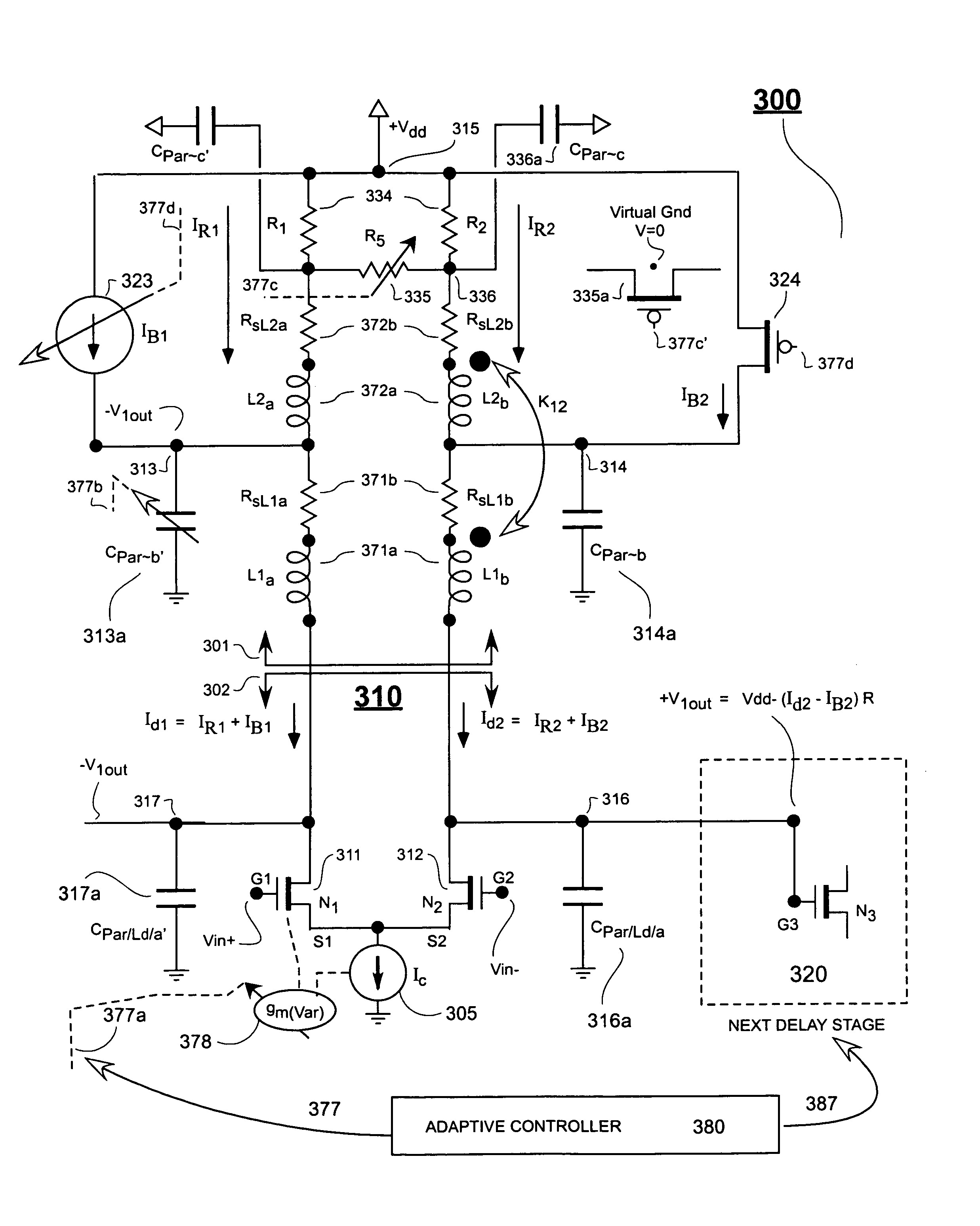
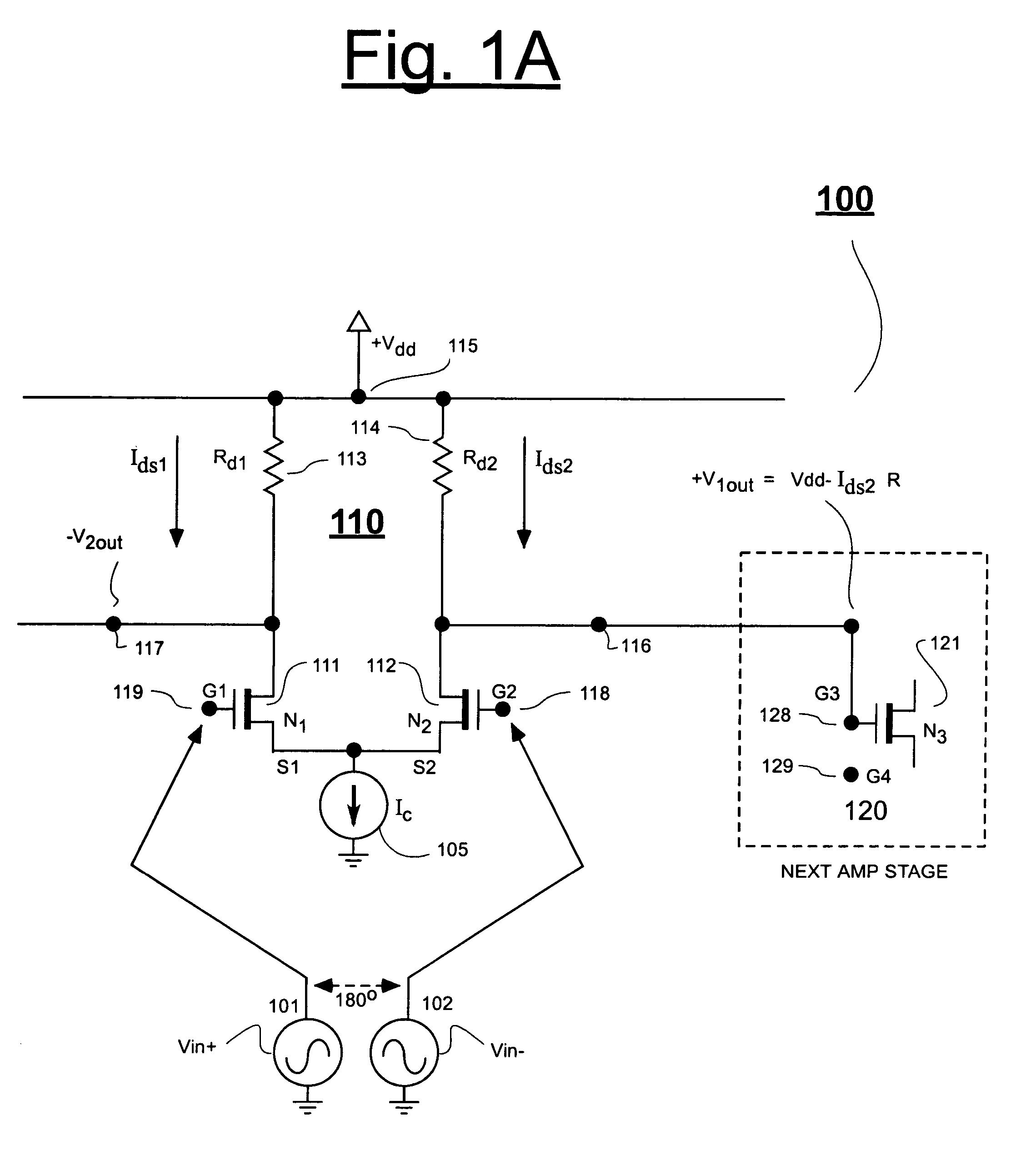
[0025]FIG. 1A shows a classical combination 100 of series cascaded, differential amplifiers such as amplifiers 110 and 120. The first differential amplifier 110 is defined by twin, N-channel transistors 111 and 112, and by a common current sink 105 coupled to their source nodes, S1 and S2. Drain load resistors 113 and 114 respectively couple to the drain nodes of transistors 111 (N1) and 112 (N2) and also to a power supply node 115 which provides a supply voltage, +Vdd. Part of the next differential amplifier 120 is shown with the gate node G3 of its transistor 121 (N3) being directly connected to the drain output node 116 of transistor 112 (N2). The drain output voltage, +V1out, of transistor 112 (N2) thus becomes the gate input voltage of next transistor 121 (N3).
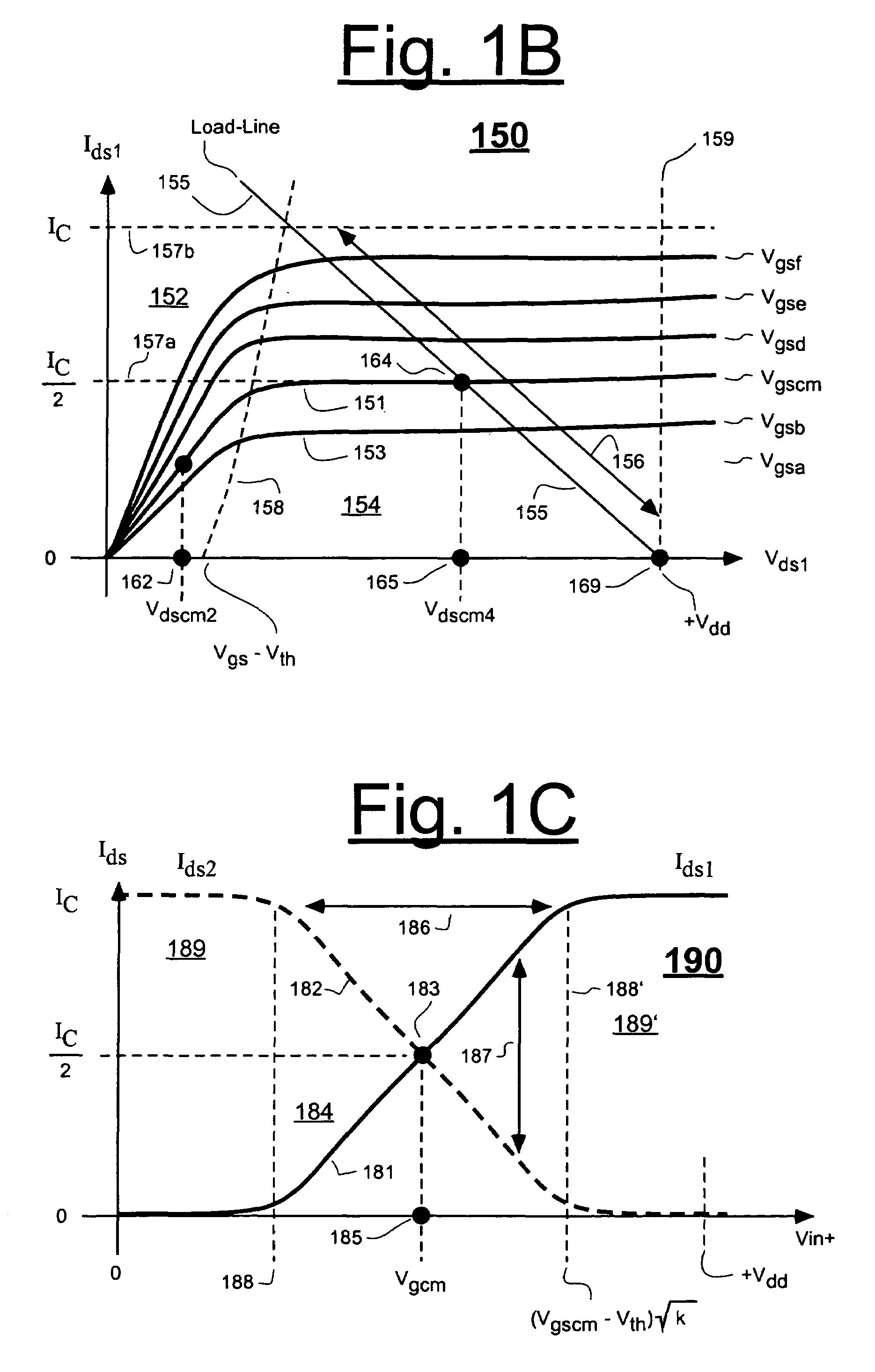
[0026]The magnitude of the first drain output voltage, +V1out, may be defined as Vdd−Ids2·Rd2, where Ids2 is the drain current of transistor 112 (N2), and Rd2 is the drain load of the same transistor 112 (N2). The magnitu...
PUM
 Abstract
Description
Claims
Application Information