

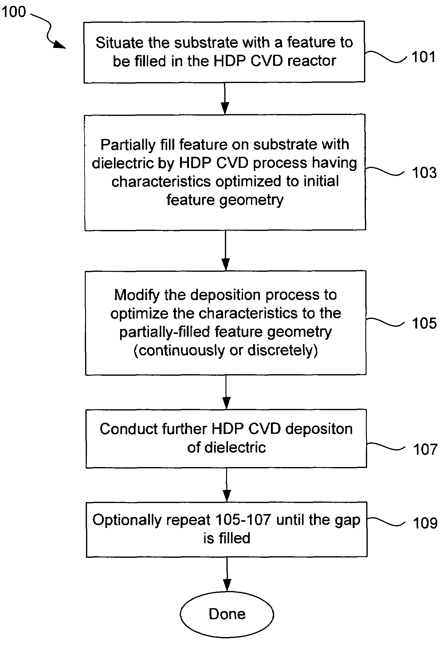
Dynamic modification of gap fill process characteristics
a technology of process characteristics and dielectrics, applied in the direction of chemical vapor deposition coating, semiconductor/solid-state device testing/measurement, coatings, etc., can solve the problems of reducing budgets, void-free filling of high aspect ratio spaces (ar>3.0:1) becomes increasingly difficult, and the dielectric deposited on the sidewall of the trench can be reduced relative to the deposited at the bottom, and the effect of optimal minimization
- Summary
- Abstract
- Description
- Claims
- Application Information
AI Technical Summary
Benefits of technology
Problems solved by technology
Method used
Image

Examples
example 1
Performance of Dynamically Modified Process Vs. Process Operating at Constant Settings Using Direct Measurement
[0061]Gap fill of a structure 500 Å wide by 3000 Å deep using a process operating at constant settings resulted in voids. The voids were eliminated by using a 2-step process to fill a feature of the same dimensions. The process characteristics were modified based on the changed feature geometry determined by direct measurement following the first deposition step. The first step had a deposition rate of 1000 A / min and a SD ratio of 0.1. The second step had a deposition rate of 5500 Å / min and a SD ratio of 0.17. Uniform performance for both the center and edge of the wafer was demonstrated.
example 2
Design of Experiment for Process Modification Based on Evolving Feature Geometry
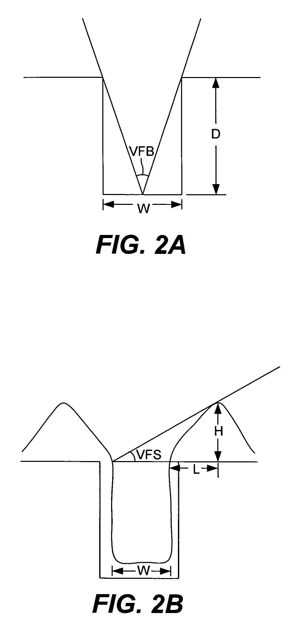
[0062]A design of experiment was carried out using structures of controlled geometry. The local growth rates at various locations in the trench were correlated to the characteristics of the process (DR, SER) and the geometry of the structure to generate a model response:[0063]Normalized growth rate w / trench Bottom=0.61+0.031−DR+0.40−SER+0.17−VFB−0.16−VF side−0.27−SER−VF side+0.26−SER VF side−0.16−VFB−VF side[0064]Normalized side max rate=0.20−0.076−DR+0.037−SER−0.049−VFB−0.024−VF Side−+0.049−DR−VFB[0065]Sidewall max: Bottom Ratio=0.21−2.146 E−3.DR[0066]+0.063−SER−0.063−VFB−0.038 VF side[0067]+0.094 DR. VF side+0.056−VFB−FV Side[0068]DR=deposition rate on monitor wafer[0069]SER=sputter rate on monitor wafer
[0070]The results, when plotted as shown if FIGS. 3A and B above, demonstrate that in order to keep the sidewall:bottom growth ratio (and gap-fill performance) constant as the trench fills, the sputter ...
PUM
| Property | Measurement | Unit |
|---|---|---|
| Temperature | aaaaa | aaaaa |
| Temperature | aaaaa | aaaaa |
| Pressure | aaaaa | aaaaa |
Abstract
Description
Claims
Application Information