High output impedance charge pump for PLL/DLL

a charge pump and high output technology, applied in the direction of pulse automatic control, electric devices, etc., can solve the problems of phase error, significant static phase error, and static phase error increase as the technology is smaller, so as to minimize the static phase error of the charge pump, reduce the effect of low power supply voltage and reduce the effect of static phase error

Active Publication Date: 2007-02-13
MOSAID TECH
View PDF10 Cites 30 Cited by
  • Summary
  • Abstract
  • Description
  • Claims
  • Application Information

AI Technical Summary

Benefits of technology

[0016]The static phase error in a charge pump is minimized through the use of an active current source. The active current mirror also mitigates the effects of low power supply voltage. According to an embodiment of the invention, a charge pump includes a pull-up circuit, a pull-down circuit and an operational amplifier. The pull-up circuit supplies a pull-up current to increase voltage at the charge pump output. The pull-down circuit supplies a pull-down current to decrease voltage at the charge pump output. The operational amplifier has a first input and a second input. The first input is coupled to the charge pump output and the second input coupled to a drain of a transistor that supplies current to the pull-down circuit. The operational amplifier output is coupled to the transistor and the pull-down circuit. The operational amplifier adjusts the voltage level at the operational amplifier output so that the voltage difference between the operational amplifier inputs is minimized and the difference between the pull-down current and the pull-up current is decreased.

Problems solved by technology

The difference in current between transistor 215 and transistor 210 can be as large as about 20% which results in a significant static phase error when the DLL is in lock condition.
In the embodiment shown, the static phase error increases as technologies become smaller because the output impedance of transistors becomes smaller.
Therefore the phase error is present by the inherent design of the prior art DLL.
In submicron technologies (i.e., 0.13 microns and smaller) the output impedance of a transistor decreases as the channel length shrinks, so the transistors do not meet the requirements for the output impedance required for an output transistor of a charge pump.
However, a cascode current source does not fit well with the trend of power supply voltage decrease.

Method used


Image

  • High output impedance charge pump for PLL/DLL
  • High output impedance charge pump for PLL/DLL
  • High output impedance charge pump for PLL/DLL

Examples


Embodiment Construction

[0031]A description of preferred embodiments of the invention follows.

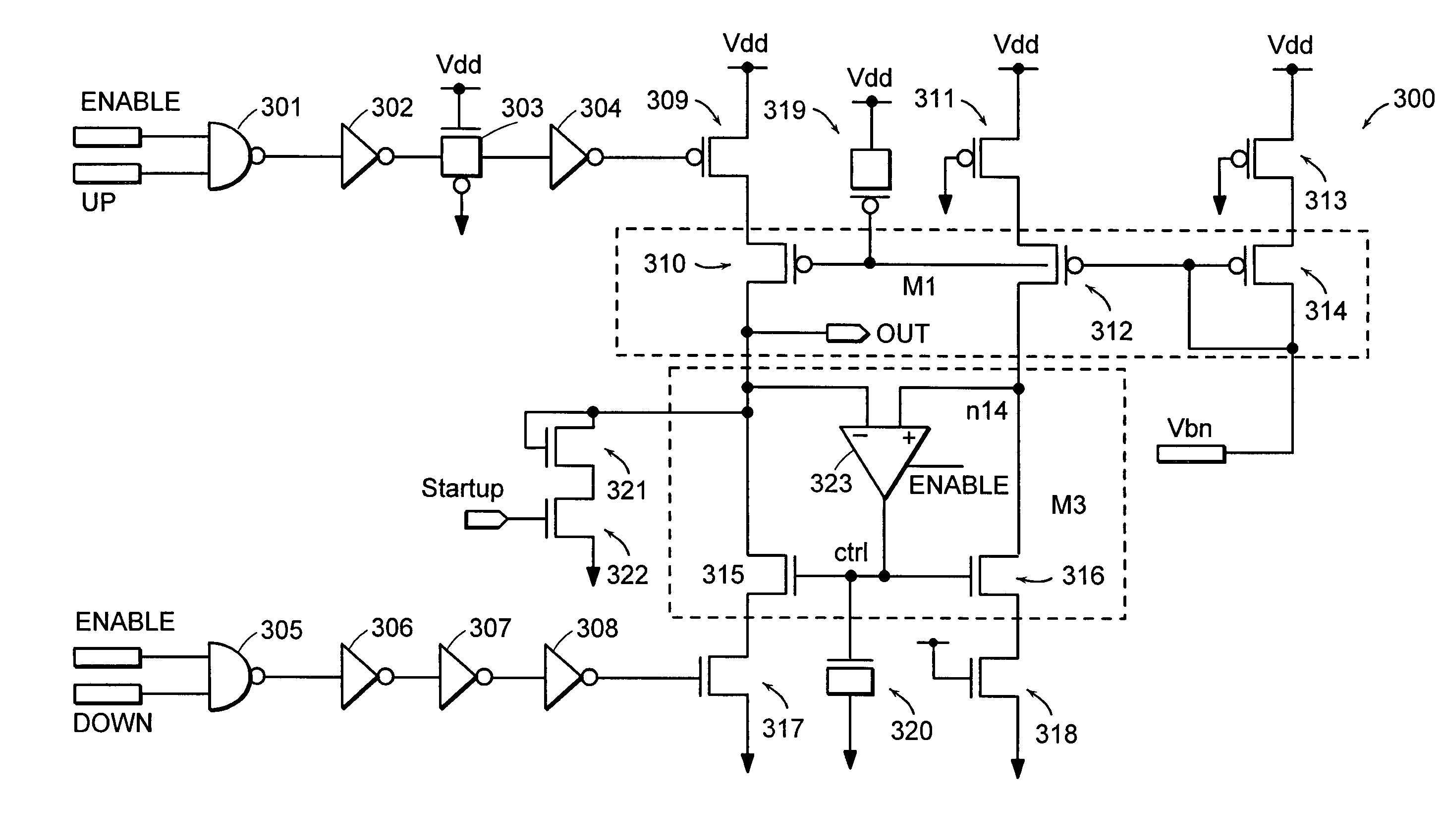
[0032]FIG. 4 is a schematic of a charge pump 300 according to the principles of the present invention. The charge pump 300 includes a plurality of transistors. In the embodiment shown, the transistors are metal-oxide semiconductor (“MOS”) transistors, also referred to as field effect transistors (“FET”). As is well-known to those skilled in the art, there are two types of MOS transistors: n-channel MOS transistors (NMOS) and p-channel MOS transistors (PMOS). The charge pump 300 includes both NMOS and PMOS transistors. The PMOS transistors are graphically illustrated with a circle at the gate.

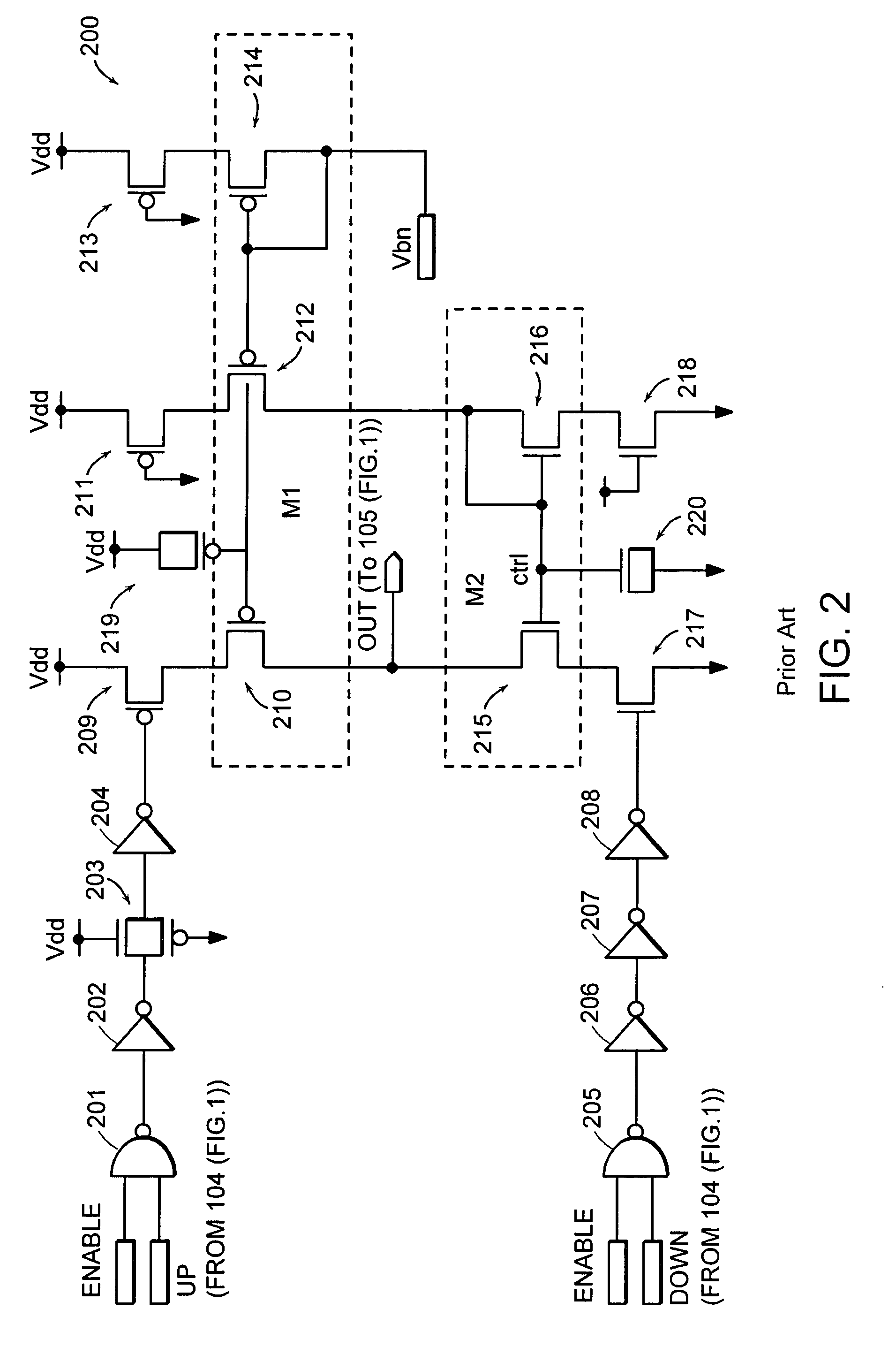
[0033]The charge pump 300 includes current mirror M1 and active current mirror M3. Current mirror M1 is similar to the current mirror M1 described in conjunction with the prior art charge pump 200 shown in FIG. 2. The active current mirror M3 includes an operational amplifier (“op amp”) 323 which minimizes static phase error b...


PUM


Abstract

A charge pump for use in a Phase Locked Loop / Delay Locked Loop minimizes static phase error through the use of an operational amplifier. The operational amplifier also mitigates the effects of low power supply voltage.

Description

RELATED APPLICATION[0001]This application claims the benefit of U.S. Provisional Application No. 60 / 528,958, filed on Dec. 11, 2003. The entire teachings of the above application are incorporated herein by reference.BACKGROUND OF THE INVENTION[0002]A Delay Locked Loop (DLL) with an adjustable delay line is used to synchronize a first clock signal with a second clock signal by delaying the first clock signal. The DLL includes a phase detector, which detects the phase difference between the first clock signal and the second clock signal. Based on the detected phase difference, the DLL synchronizes the first clock signal to the second clock signal by adding an appropriate delay to the first clock signal until the second clock signal is in phase with the first clock signal.[0003]FIG. 1 is a block diagram of a prior art DLL 100. An externally supplied clock (CLK) is buffered by clock buffer 101 to provide a reference clock (CLK_REF) that is coupled to a voltage controlled delay line 102 ...

Claims


Application Information

Patent Timeline
Patent Type & Authority Patents(United States)
IPC IPC(8): H03L7/06H03L7/00H03L7/08H03L7/081H03L7/089
CPCH03L7/0895H03L7/0812H03L7/0816H03L7/08H03L7/093H03L7/06
Inventor HAERLE, DIETER
Owner MOSAID TECH
Why Eureka
Try Eureka