Electron-emitting device, electron-emitting apparatus, image display apparatus, and light-emitting apparatus

a technology of electron-emitting devices and electron-emitting devices, which is applied in the manufacture of electrode systems, electric discharge tubes/lamps, and screens with screens, etc., can solve the problems of increasing the power consumption of driving due to the device capacitance of electron-emitting devices, increasing the requirement for higher resolution of image display apparatuses, and high voltage. , to achieve the effect of high-luminance emission/display, low vacuum degree, and increased ra

Inactive Publication Date: 2007-03-06
CANON KK
View PDF149 Cites 12 Cited by
  • Summary
  • Abstract
  • Description
  • Claims
  • Application Information

AI Technical Summary

Benefits of technology

[0036]The electron-emitting device of the present invention can stably emit electrons in a low vacuum degree at an increased rate for a long time period.
[0037]According to the present invention, a light-emitting member is provided on the anode in the electron-emitting apparatus or above the electron-emitting device to form a light-emitting device, an image display apparatus or the like capable of operating in a low vacuum degree and effecting high-luminance emission / display for a long time period with stability.

Problems solved by technology

In recent years, however, there has been a tendency to require higher resolution of image display apparatuses.
Further, with the increase in the number of display pixels, power consumption during driving due to the device capacitance of electron-emitting devices is increased.
Moreover, the drive voltage is high, several ten to several hundred volts, and capacitive power consumption is disadvantageously large because of the specific structure.
This method, however, has the problem of an increase in complexity of the manufacturing process, a reduction in electron emission efficiency, etc., due to the addition of the focusing electrode.
Therefore the structure of lateral FE electron sources has the problem of a reduction in the efficiency (the ratio of the electron current flowing through the gate and the electron current reaching the anode) and considerable spreading of the beam shape on the anode.

Method used


Image

  • Electron-emitting device, electron-emitting apparatus, image display apparatus, and light-emitting apparatus
  • Electron-emitting device, electron-emitting apparatus, image display apparatus, and light-emitting apparatus
  • Electron-emitting device, electron-emitting apparatus, image display apparatus, and light-emitting apparatus

Examples


embodiment 1

(Embodiment 1)

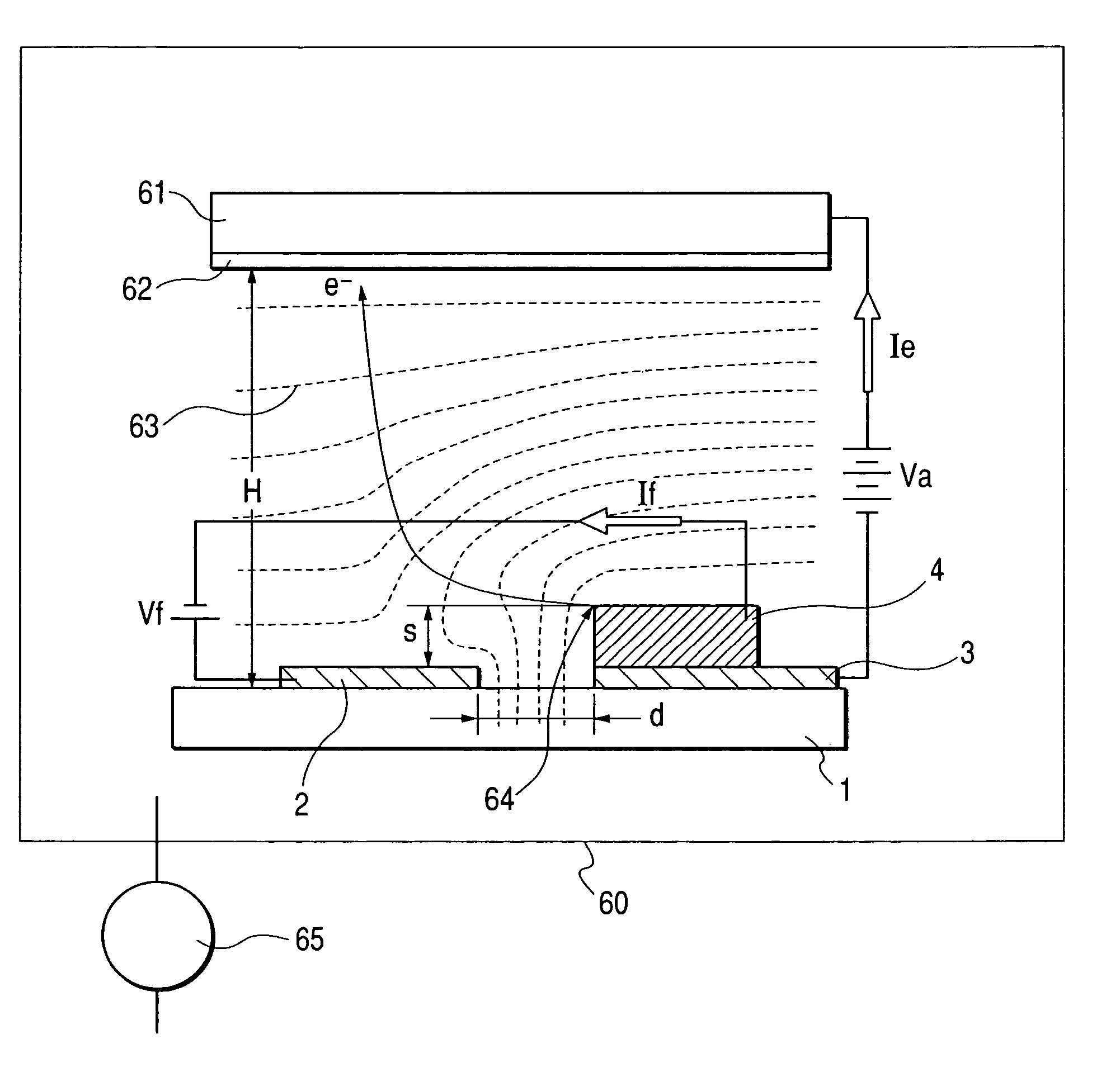
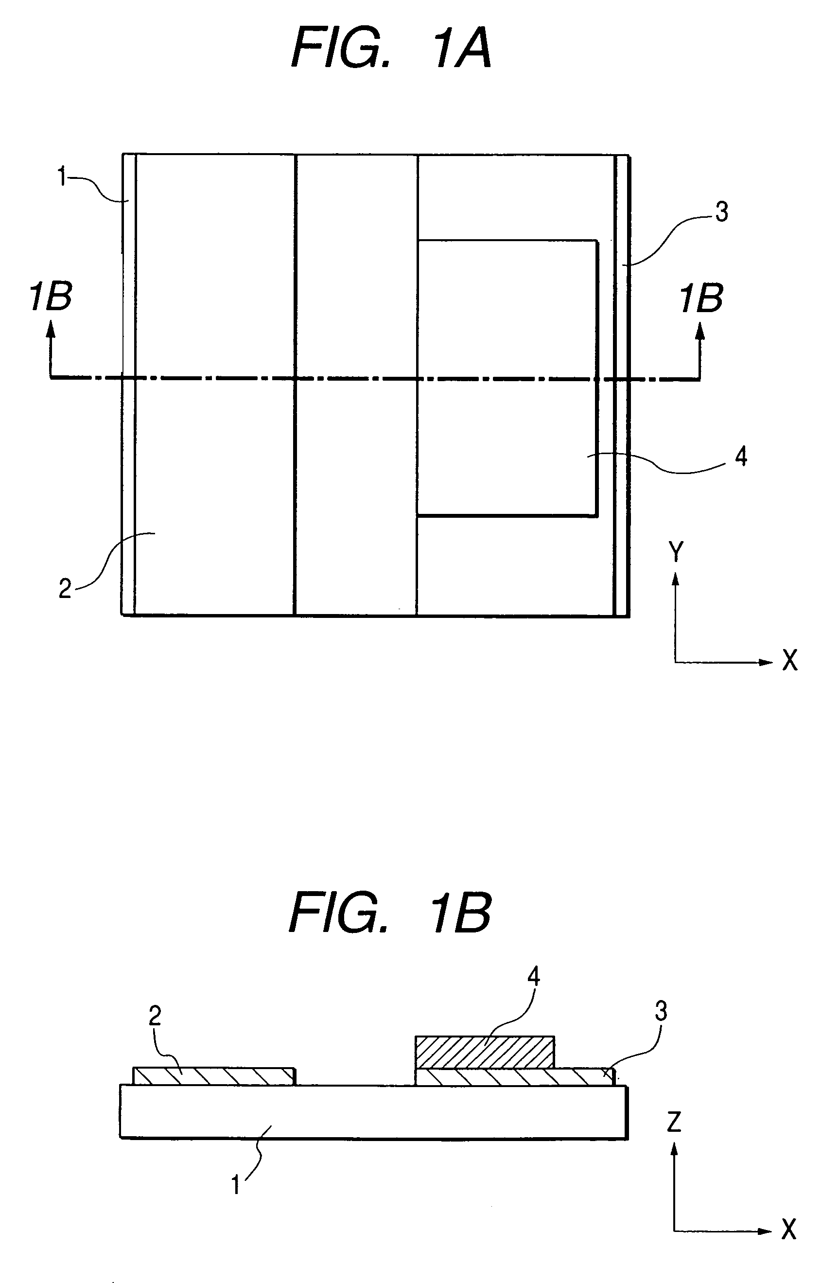
[0128]FIG. 1A shows a top view of an electron-emitting device fabricated in this embodiment. FIG. 1B is a cross-sectional view taken along the line 1B—1B of FIG. 1A.

[0129]FIGS. 1A and 1B illustrate an insulating substrate 1, an extraction electrode 2 (gate), a cathode 3, and an emitter material 4.

[0130]The process of fabricating the electron-emitting device of this embodiment will be described in detail.

(Step 1)

[0131]A quartz substrate was used as substrate 1. After sufficiently cleansing the substrate, a 5 nm thick Ti film (not shown) and a 30 nm thick poly-Si film (arsenic doped) were successively deposited by sputtering on the substrate as gate electrode 2 and cathode 3.

[0132]Next, a resist pattern was formed by photolithography using a positive photoresist (AZ1500 / from Clariant Corporation).

[0133]Thereafter, dry etching was performed on the poly-Si (arsenic doped) layer and Ti layer with the patterned photoresist used as a mask, CF4 gas being used to etch the Ti l...

embodiment 2

(Embodiment 2)

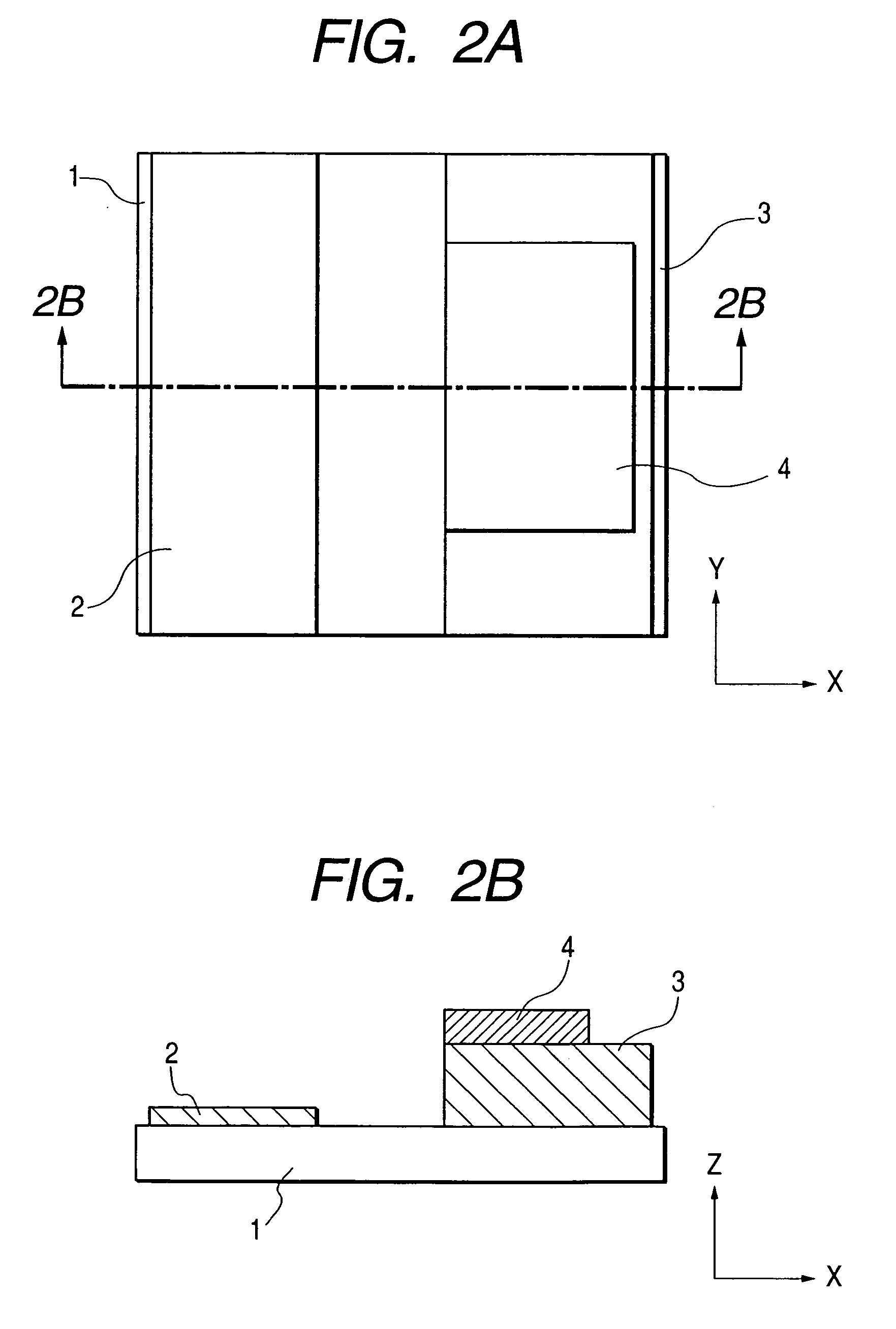
[0147]FIG. 2 shows a second embodiment of the present invention.

[0148]In this embodiment, an electron-emitting device was fabricated in the same manner as that in the first embodiment except that the cathode 3 corresponding to that in the first embodiment had a thickness of 500 nm and fibrous carbon provided as electron-emitting material 4 had a thickness of 100 nm. Currents If and Ie in the fabricated electron-emitting device were measured.

[0149]In this device arrangement, the electron emission point was positively heightened (toward the anode) relative to the gate electrode by increasing the thickness of the cathode 3. Trajectories along which electrons impinge on the gate were thereby reduced, thereby preventing a reduction in efficiency and occurrence of a beam-thickening phenomenon.

[0150]Also in this device arrangement, the electron emission current Ie at Vf=20V was about 1 μA. On the other hand, the If characteristic was similar to the Ie characteristic but the v...

embodiment 3

(Embodiment 3)

[0152]FIG. 3 shows a third embodiment of the present invention.

[0153]In this embodiment, in the step corresponding to step 2 in the first embodiment, palladium oxide 51 was provided on the cathode 3 and in the gap between the electrodes 2 and 3. Pd oxide was provided in the gap in such a manner as to extend from the cathode 3 to a point near the midpoint of the gap. Excepting step 2, this embodiment is the same as the first embodiment.

[0154]The electric field in the electron-emitting device of this embodiment was twice as strong as that in the first embodiment because the gap was reduced, thereby enabling the drive voltage to be reduced to about 8 V.


PUM


Abstract

An electron-emitting device in which the specific capacitance and the drive voltage are reduced, and which is capable of obtaining a finer electron beam by controlling the trajectory of emitted electrons. An electron-emitting portion of an electron-emitting member is positioned between the height of a gate and the height of an anode. When the distance between the gate and a cathode is d; the potential difference at driving the device is V1; the distance between the anode and the substrate is H; and the potential difference between the anode and the cathode is V2, then the electric field E1=V1/d during driving is configured to be within the range from 1 to 50 times E2=V2/H.

Description

[0001]This application is a division of U.S. application Ser. No. 09 / 941,780, filed Aug. 30, 2001.BACKGROUND OF THE INVENTION[0002]1. Field of the Invention[0003]The present invention relates to an electron-emitting device, an electron-emitting apparatus, an electron source and an image-forming apparatus. The present invention also relates to a display apparatus such as a television broadcast display, a display for use in a video conference system or a computer display, and to an image-forming apparatus designed as an optical printer using a photosensitive drum or the like.[0004]2. Related Background Art[0005]A field emission (FE) type of electron-emitting device which emits electrons from a surface of a metal when a strong electric field of 106 V / cm or higher is applied to the metal, and which is one of the known cold cathode electron sources, is attracting attention.[0006]If the FE-type cold electron source is put to practical use, a thin emissive type image display apparatus can ...

Claims


Application Information

Patent Timeline
Patent Type & Authority Patents(United States)
IPC IPC(8): H01J9/12H01J29/04H01J1/30H01J1/304H01J31/12H01J63/06
CPCB82Y10/00H01J1/304H01J2329/00H01J2201/30469C01B32/05H01J1/30
Inventor TSUKAMOTO, TAKEO
Owner CANON KK
Why Eureka
Try Eureka