Low dielectric materials and methods for making same

a technology of low dielectric materials and methods, applied in the field of materials, can solve the problems of difficult identification of improved low dielectric compositions, difficult to use these low dielectric compositions, and cracking or delamination

Inactive Publication Date: 2007-03-06
SYMYX SOLUTIONS +1
View PDF25 Cites 74 Cited by
  • Summary
  • Abstract
  • Description
  • Claims
  • Application Information

AI Technical Summary

Problems solved by technology

In some of these processes, temperature cycling of multiple layers may induce stresses due to the thermal coefficient of expansion mismatch between the different materials thereby causing cracking or delamination.
Consequently, it may be impractical to use these low dielectric compositions due to the trade-off in dielectric constant with elastic modulus.
Furthermore, it is often difficult to identify improved low dielectric compositions due to this trade-off in dielectric constant with elastic modulus.
This is a critical failing in the prior art: the inability to understand and quantify the trade-off between κ and modulus to be able to identify a material with improved performance.
However, these results were empirically derived for a given set of materials and are not generally extendible to other classes of materials.
Further, Bremmer did not teach that one value, or figure of merit, could be used to characterize each E vs. κ curve.
These impurities may result from residual levels of catalyst used in the manufacture of the chemical precursor reagents.
Such levels of residual catalytic impurities are often of little consequence in typical applications of these chemicals because the surfactant is often used at such low levels that the catalytic impurities imparted by the surfactant become insignificant in the final formulation.
A further source of impurities may result from an inattention to detail, such as packaging or handling outside a clean room, because such stringent purity requirements are not needed for typical applications.
The reference, US 2002 / 0045693, discusses how the dielectric properties of the resulting films may be adversely affected by the purification of reagents even if surfactant is not present.
The cure or anneal step, in which the coated substrate is typically heated to decompose and / or remove volatile components and substantially cross-link the film, is a significant source of production bottlenecks.
Various components of IC devices such as Cu metal lines can only be subjected to processing temperatures for short time periods before their performance deteriorates due to undesirable diffusion processes.

Method used


Image

  • Low dielectric materials and methods for making same
  • Low dielectric materials and methods for making same
  • Low dielectric materials and methods for making same

Examples


example 1 – 14

Example 1–14

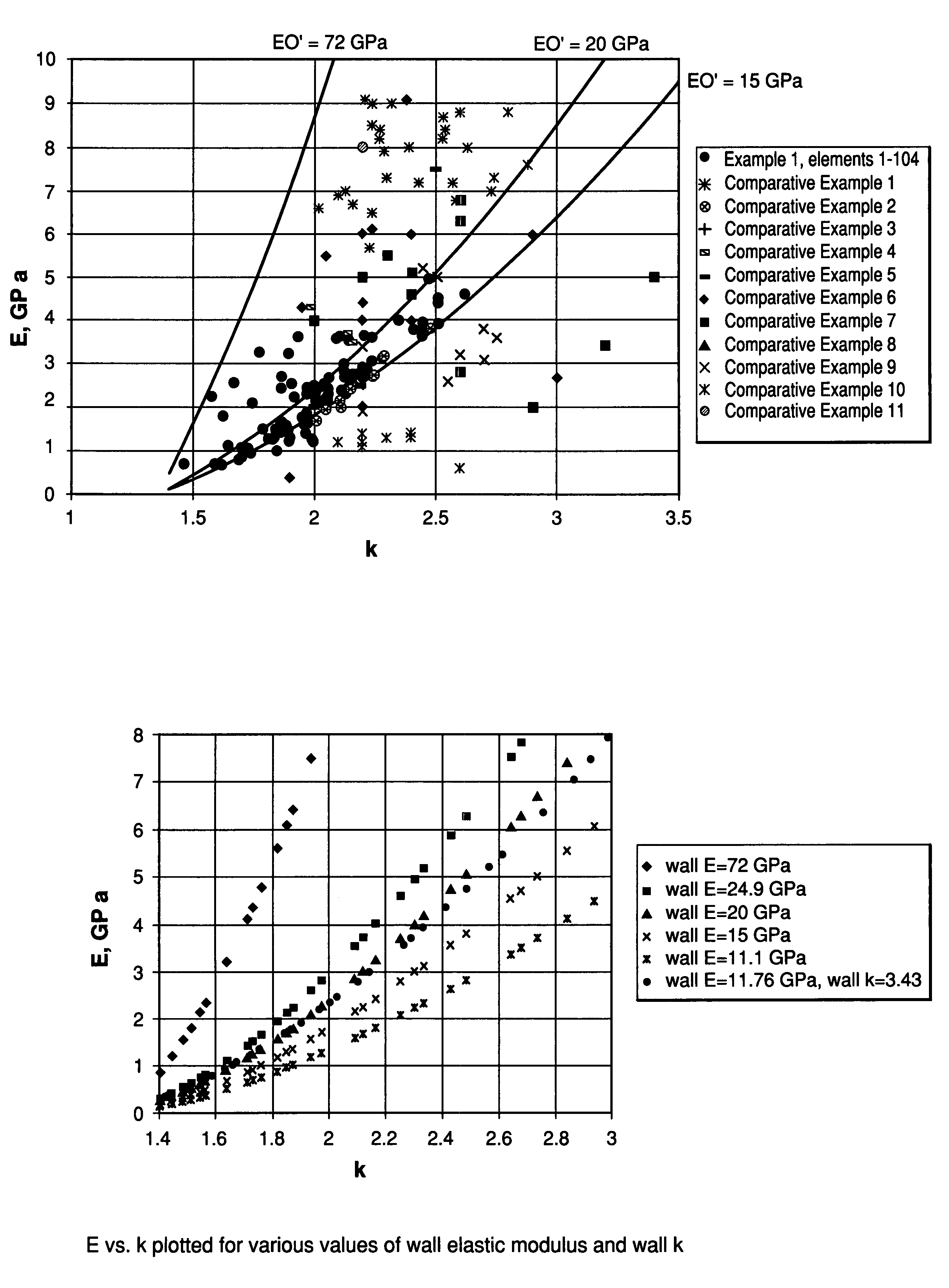
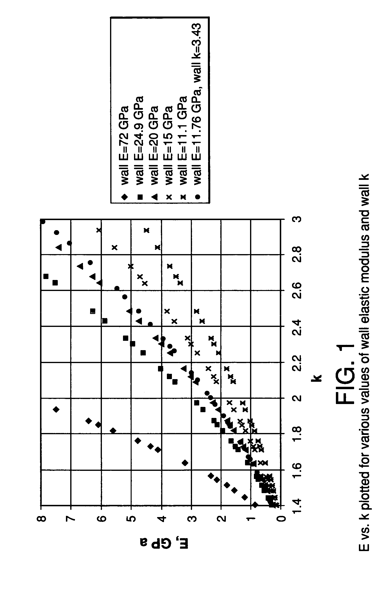
Selected Array Elements as Compartive Examples to Spun Coated Films

[0120]Sample films were prepared in the same manner as the general process for preparing array elements. The volume of each reagent dispensed into individual microtiter wells is provided in Table II. The solutions were dispensed, agitated, and calcined as in the general procedure to prepare array elements to films. The properties of each film are provided in Table III.

[0121]

TABLE IICOMPOSITION OF ARRAY ELEMENTS4:1 VolumeNitricHydrophilicHydrophobicSolvent:SurfactantWaterAcidTMAHEx.Source (μl)Source (μl)Ratio (μl)Solvent (μl)(μl)(μl)(μl)1138.2144.4 MTES329.9 PGMEA:L101573.2 PGMEA0.0247.2 0.1 M5TEOS2.4 wt. %2121.0126.2177.2207.50.0119.9 0.1 M5TEOSMTESpentanol:X114;pentanol;2.4 wt. %204.7261.8 PGMEAPGMEA:X114368.571.5163.4 PGPE:L101274.8 PGPE93.726.3 0.025 M5TEOSMTES1.2 wt. %468.571.5163.4 PGPE:L101274.8 PGPE58.761.2 0.2 M5TEOSMTES1.2 wt. %549.661.0189.3 PGPE:X114270.6 PGPE26.829.7 0.2 M5TEOSMTES; 9.71.2 wt....

example 15

Spin Coating

[0123]A mixture was prepared containing 317.9 μl of TEOS and 326.3 μl of MTAS. A quantity of 635.7 μl of a 4:1 volume ratio of PGPE: Triton X-45 and 2027.3 μl of PGMEA was added to the mixture. Next, additional reagents were added to the mixture in the following order: 390 μl of water, 119.6 μl of 0.025 M HNO3, and 22.8 l of 1.2 wt. % TMAH in water. After the addition of water the mixture was aged at room temperature for 5 minutes. The subsequent addition of HNO3 and TMAH were also followed by individual 5 minutes aging steps. Once all of the reagents have been added, the entire solution is aged for 5 minutes at room temperature and agitated for 2–3 minutes to thoroughly mix the solution. The resulting clear solution was then aged for 1–24 hours at room temperature prior to spin coating.

[0124]The sol was dispensed onto a low resistivity P type Si wafer spinning at 500 rpm for 7 seconds and then accelerated to 1800 rpm for 35–40 seconds. The film formed during the spin c...

examples 16 – 27

Examples 16–27

[0127]Sample films were prepared in the same manner as Example 15 except that the types and / or amounts of silane sources, surfactant, solvent, and catalyst in the mixture were varied. These variations are provided in Table IV. The properties of each film are provided in Table V.

[0128]As Table V illustrates, under some conditions, materials with high E0′ were obtained at pHs greater than about 4 or using Si sources that generate acetic acid during hydrolysis and condensation.

[0129]Comparison of Tables III and V illustrate that compositions having relatively higher normalized wall elastic modulus, produced in an array format using alternative evaporative techniques, such as an orbital movement device, can be reproduced using conventional spin coating techniques.

Array Elements 28–131:

[0130]Sample films were prepared in the same manner as Example 1 except that the types and / or amounts of silica sources, surfactant, solvent, and catalyst in the mixture were varied. These va...


PUM

PropertyMeasurementUnit
wall elastic modulusaaaaaaaaaa
dielectric constantaaaaaaaaaa
temperatureaaaaaaaaaa

Abstract

Low dielectric materials and films comprising same have been identified for improved performance when used as interlevel dielectrics in integrated circuits as well as methods for making same. These materials are characterized as having a dielectric constant (κ) a dielectric constant of about 3.7 or less; a normalized wall elastic modulus (E0′), derived in part from the dielectric constant of the material, of about 15 GPa or greater; and a metal impurity level of about 500 ppm or less. Low dielectric materials are also disclosed having a dielectric constant of less than about 1.95 and a normalized wall elastic modulus (E0′), derived in part from the dielectric constant of the material, of greater than about 26 GPa.

Description

CROSS-REFERENCE TO RELATED APPLICATIONS[0001]This application is a divisional of application Ser. No. 10 / 158,511, filed 30 May 2002, which is incorporated herein by reference in its entirety.BACKGROUND OF THE INVENTION[0002]The present invention relates generally to materials suitable for use in electronic devices. More specifically, the invention relates to materials and films comprising same having an improved elastic modulus and a low dielectric constant expressed through a higher normalized wall elastic modulus and to methods for making same.[0003]There is a continuing desire in the microelectronics industry to increase the circuit density in multilevel integrated circuit devices such as memory and logic chips in order to improve the operating speed and reduce power consumption. In order to continue to reduce the size of devices on integrated circuits, it has become necessary to use insulators having a low dielectric constant to reduce the resistance-capacitance (“RC”) time dela...

Claims


Application Information

Patent Timeline
Patent Type & Authority Patents(United States)
IPC IPC(8): H01L21/8242H01L29/94C01B33/16H01L21/768H01B3/12H01B3/46H01L21/312H01L21/316H01L23/522
CPCC09D183/04H01L21/02126H01L21/31695H01L21/02282H01L21/02203Y10T428/249979Y10T428/249967Y10T428/249969H01B3/12C01B33/16
Inventor KIRNER, JOHN FRANCISMACDOUGALL, JAMES EDWARDPETERSON, BRIAN KEITHWEIGEL, SCOTT JEFFREYDEIS, THOMAS ALANDEVENNEY, MARTINRAMBERG, C. ERICCHONDROUDIS, KONSTANTINOSCENDAK, KEITH
Owner SYMYX SOLUTIONS
Why Eureka
Try Eureka