Method of fabrication of a support structure for a semiconductor device

a technology of support structure and semiconductor device, which is applied in the direction of semiconductor laser structure details, crystal growth process, semiconductor laser, etc., can solve the problems of high doping level, low defect density, and normal substrate growth methods such as vgf (vertical gradient freeze) techniques, so as to achieve optimum device performance, minimize optical absorption, and low defect density

Inactive Publication Date: 2007-03-13
ARASOR ACQUISITION +1
View PDF10 Cites 10 Cited by
  • Summary
  • Abstract
  • Description
  • Claims
  • Application Information

AI Technical Summary

Benefits of technology

[0010]In one embodiment of the invention, the doping of the grown semiconductor layer is uniform and can be selected for optimum device performance. Low defect density is achieved as described above and is fully decoupled from the doping density. In a second embodiment, the doping density is not uniform. For example, it might be kept very low (less than 1×1016 cm−3) through most of the grown layer to minimize optical absorption and increased only in a thin region close to the active devices to provide good electrical conduction.

Problems solved by technology

Normal methods of substrate growth, such as the VGF (vertical gradient freeze) technique, can only achieve low defect densities if the doping level is high (greater than 1×1018 cm−3 in GaAs, for example).
Such high doping levels are usually undesirable for bottom emitting VCSELs or NECSELs as described above.

Method used


Image

  • Method of fabrication of a support structure for a semiconductor device
  • Method of fabrication of a support structure for a semiconductor device
  • Method of fabrication of a support structure for a semiconductor device

Examples


first embodiment

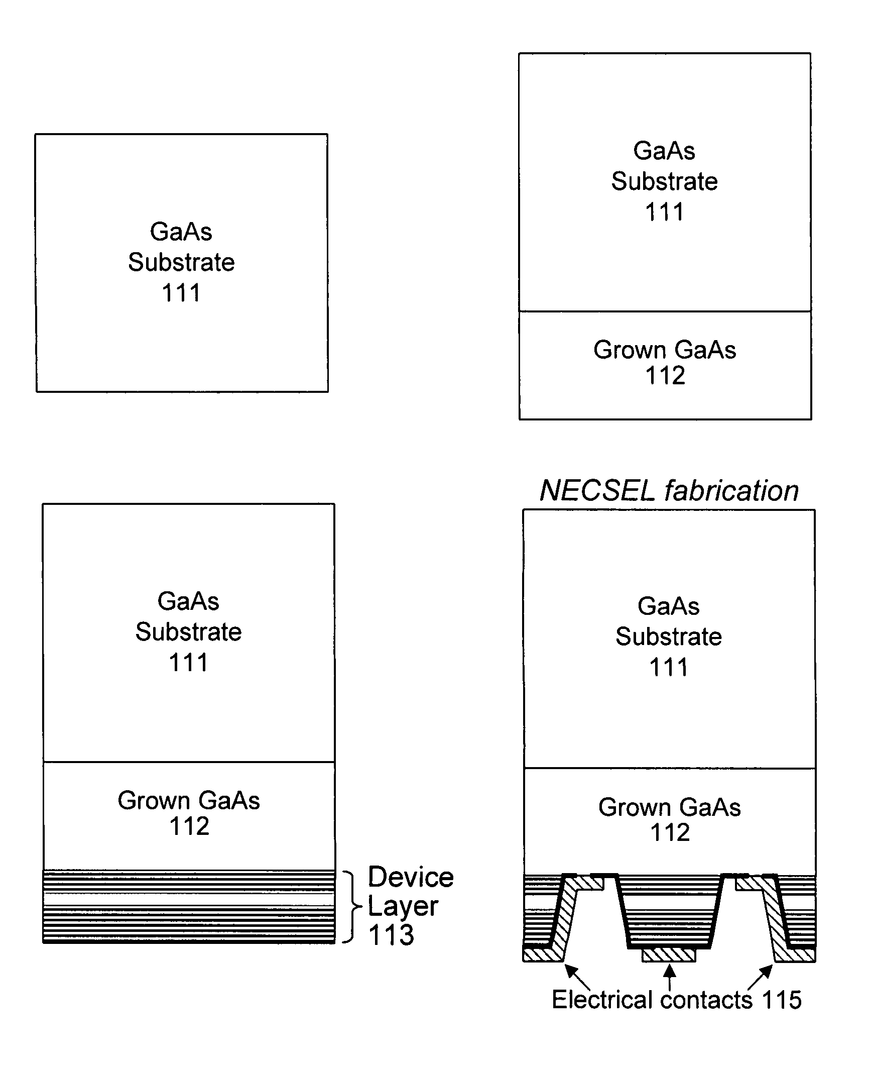
[0019]According to the present invention, the support layer 112 has a uniform doping level of between 5×1016 cm−3 and 5×1017 cm−3 and a thickness of about 100 μm.

second embodiment

[0020]According to the present invention, the support layer 112 is doped very lightly through most of the material (for example, less than 1×1016 cm−3) in order to minimize optical absorption, while a thin (e.g., 2 to 20 μm thick) layer of more heavily doped material (for example, 5×1017 cm−3 and 5×1018 cm−3) is formed immediately adjacent to the device layer to provide electrical conduction. Such a tailored doping profile is readily obtained, for example, by adjusting dopant source flow rates during epitaxial growth by metal organic chemical vapor deposition (MOCVD).

[0021]The effect of tailoring the doping profile in this way can be described in more detail with respect to FIGS. 3A and 3B . The figures show the modeled wall plug efficiency (WPE) for various NECSEL designs. The wall plug efficiency is the ratio of the optical power emitted by the NECSEL to the input electrical power and is an important performance value for diode lasers. In general, high wall plug efficiency is desi...


PUM

PropertyMeasurementUnit
thicknessaaaaaaaaaa
thickaaaaaaaaaa
diameteraaaaaaaaaa

Abstract

A method of fabricating a semiconductor device is described. In this method, a starting substrate of sufficient thickness is selected that has the required defect density levels, which may result in an undesirable doping level. Then a semiconductor layer having a desired doping level is formed on the starting substrate. The resulting semiconductor layer has the required defect density and doping levels for the final product application. After active components, electrical conductors, and any other needed structures are formed on the semiconductor layer, the starting substrate is removed leaving a desired thickness of the semiconductor layer. In a VECSEL application, the active components can be a gain cavity, where the semiconductor layer has the necessary defect density and doping levels to maximize wall plug efficiency (WPE). In one embodiment, the doping of the semiconductor layer is not uniform. For example, a majority of the layer is doped at a low level and the remainder is doped at a much higher level. This can result in improved WPE at particular thicknesses for the higher doped material.

Description

BACKGROUND OF THE INVENTION[0001]This application claims priority to U.S. Provisional Application 60 / 434,671 filed on Dec. 20, 2002.[0002]The present invention pertains to the fabrication of a semiconductor device or an integrated circuit (IC). More particularly, the present invention pertains to the fabrication of a device or IC through the extensive growth of a semiconductor layer of a desired doping profile and defect density on a conventional wafer.[0003]Electronic devices and integrated circuits, and methods for their fabrication, are well known in the art. Typically, the fabrication process starts with a semiconductor substrate with a suitable doping level and defect density. The elements of the device or circuit are then formed on or just below the surface of the substrate through additive processes (such as material deposition using such techniques as chemical vapor deposition (CVD) or sputtering), subtractive processes (such as etching) or processes that modify the properti...

Claims


Application Information

Patent Timeline
Patent Type & Authority Patents(United States)
IPC IPC(8): H01L21/00C30B1/00H01L21/20H01L21/36H01L33/00H01S5/02H01S5/183H01S5/323
CPCH01S5/323H01S5/18305H01S5/141H01S5/0224H01L21/02546H01L21/02395H01S5/0217H01L21/02543H01L33/0079H01L33/0093H01S5/0234
Inventor CAREY, GLEN PHILLIPJENKS, IANLEWIS, ALANLUJAN, RENEZHOU, HAILONGTITUS, JACY R.YOFFE, GIDEON W.EMANUEL, MARK A.MOORADIAN, ARAM
Owner ARASOR ACQUISITION
Why Eureka
Try Eureka