CMOS device integration for low external resistance

a technology of low external resistance and integrated circuit, which is applied in the field of complementary metal oxide semiconductor (cmos) devices with a lower external resistance, can solve the problems of low resistance/high current interconnection, reducing the external resistance of the device, and reducing the performance benefit achieved through scaling, etc., and achieves the effect of low resistance p

Inactive Publication Date: 2007-03-13
GLOBALFOUNDRIES INC
View PDF27 Cites 6 Cited by
  • Summary
  • Abstract
  • Description
  • Claims
  • Application Information

AI Technical Summary

Benefits of technology

[0022]One embodiment of the present invention is directed to a method for producing a low resistance N-type doped Field Effect Transistor (NFET) device. Doping a Si-containing substrate with a group V element of the Periodic Table of Elements typically produces an NFET device. When producing a low resistance NFET device incorporating first silicide regions, predoping of the gate can be implemented. Following gate pre-doping, a second implant forms source / drain extension regions. Finally, deep source / drain regions are formed using a further implant.
[0023]A second embodiment of the present invention is directed to a method for producing a low resistance P-type doped field effect transistor (PFET) device. PFET devices are typically produced within Si-containing substrates by doping the substrate with a group III-A element of the Periodic Table of Elements. In addition to producing low resistance PFET devices incorporating first silicide regions using one implant for the source / drain extensions and a second implant for the deep / source drain regions, it is possible to produce both the source / drain extensions and the deep source / drain regions using a single implant.

Problems solved by technology

One of the primary challenges to MOSFET scaling is lowering the device's external resistance (Rext), also known as source / drain resistance.
When scaling MOSFET devices, and if the device gate-length and the gate oxide thickness are reduced and the external resistance is held constant, then the performance benefits achieved through scaling will be limited.
First, conventional MOSFET designs utilize thick silicide layers for reducing the sheet resistance between the devices incorporated in the chip's design. The thicker the silicide, the greater the cross-section of the interconnect, resulting in a low resistance / high current interconnect. Thick silicides form into the substrate in both horizontal and vertical directions during anneal processing steps and therefore must have appropriate spacing away from the extension edge at the channel-end tip and the extension edge at the bottom of the junction.
Thick silicide regions can give rise to a substantial degree of interface roughness, which can lead to punch-through of the thin extension junctions.
Punch-through can lead to excessive level of junction leakage.
Short channel effects are well known to those skilled in the art as a decrease in threshold voltage, Vt, due to electrical charge sharing between the gate and the source drain regions, resulting in degradation of the devices ability to control whether the device is on or off.

Method used


Image

  • CMOS device integration for low external resistance
  • CMOS device integration for low external resistance
  • CMOS device integration for low external resistance

Examples


Embodiment Construction

[0033]The present invention, which provides a method of fabricating a low external resistance MOSFET device as well as the MOSFET structure formed by the inventive method, will now be described in more detail by referring to the drawings that accompany the present application. It is noted that in the accompanying drawings, like reference numerals are used for describing like and corresponding elements.

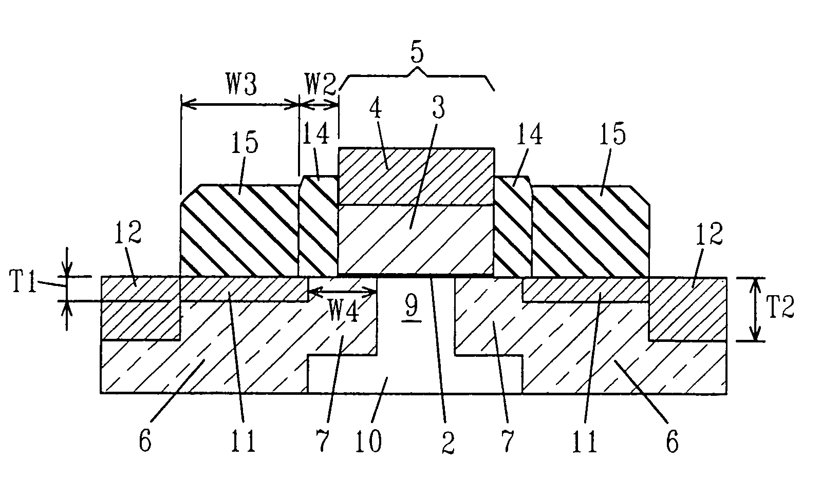
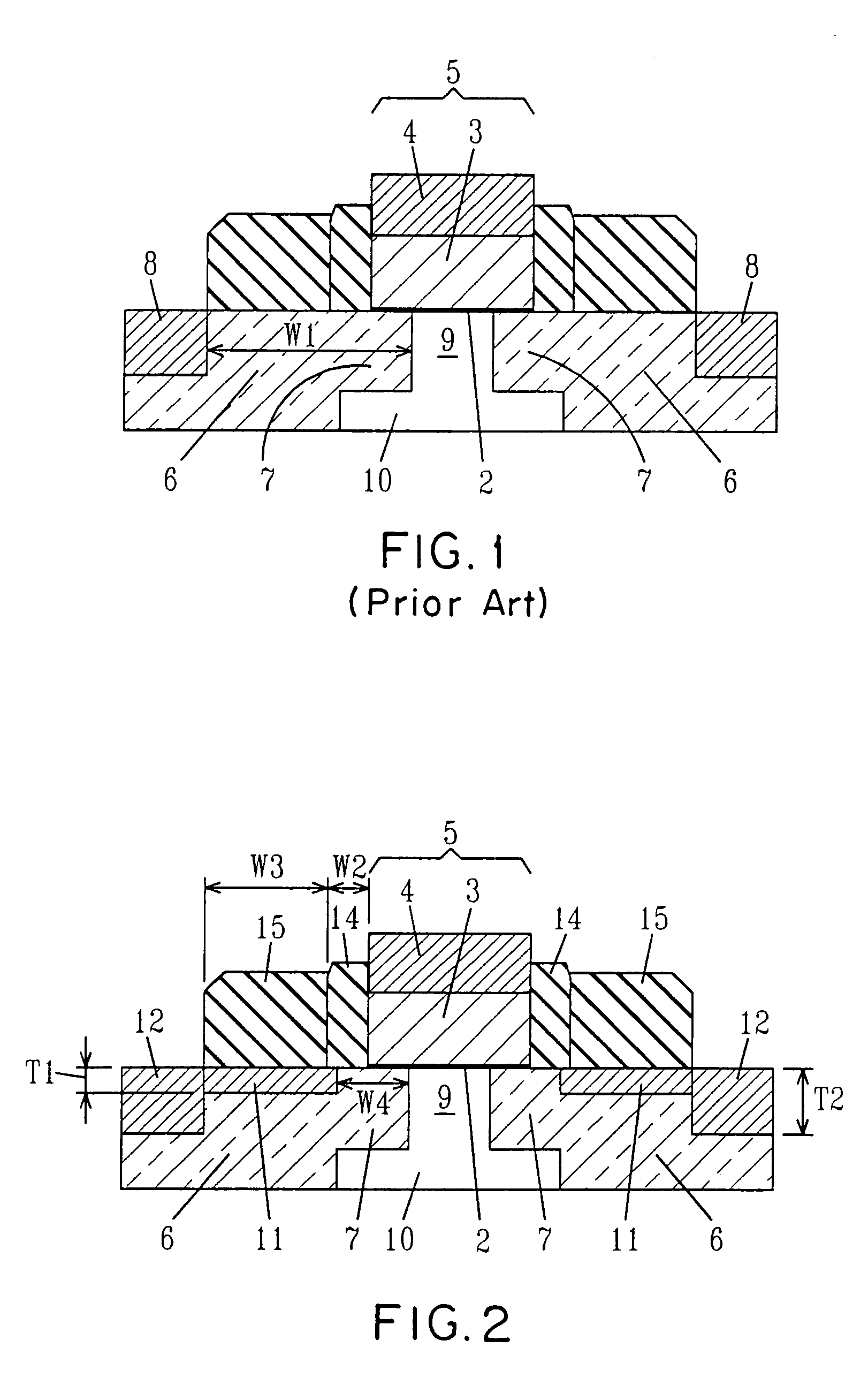
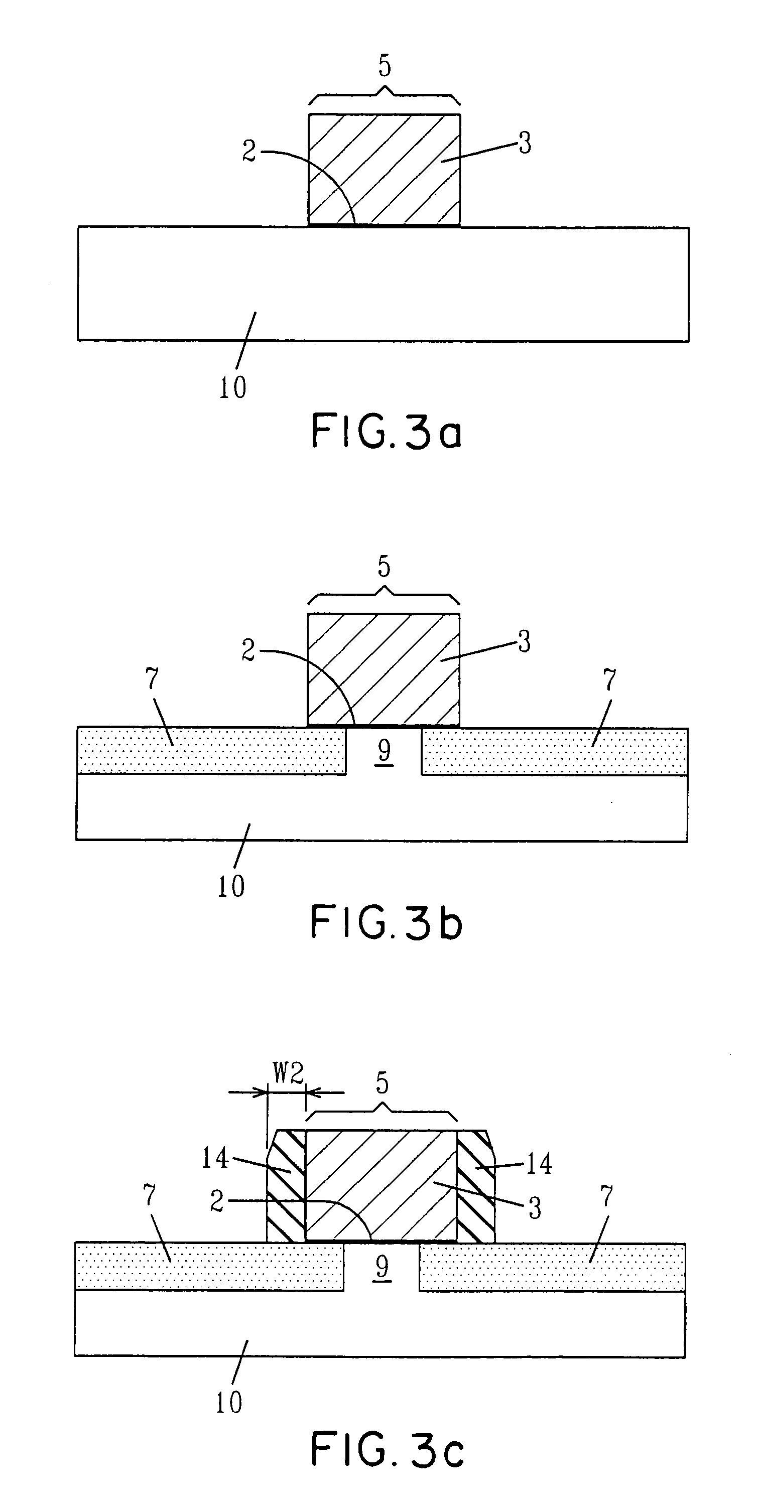
[0034]Reference is first made to FIG. 2, which depicts the MOSFET device of the present invention. The inventive MOSFET device, includes a first silicide region 11 having a first silicide thickness T1, and a second silicide region 12 having a second silicide thickness T2, where the second silicide thickness T2 is greater than the first silicide thickness T1. The inventive MOSFET device also includes a gate region 5 positioned atop a substrate 10. The gate region 5 includes a gate dielectric 2; a gate conductor 3 having sidewalls protected by an oxide layer (not specifically labeled) po...


PUM


Abstract

The present invention relates to a Complementary Metal Oxide Semiconductor (CMOS) device having a lower external resistance and a method for manufacturing the CMOS device. The inventive MOSFET is produced by forming first suicide regions in a substrate as well as atop surface of a gate region and forming second silicide regions where second silicide thickness is greater than the first silicide thickness. The inventive method produces a low resistance first silicide in close proximity to the channel region of the device, where the incorporation of the first silicide decreases the external resistance of the device while the incorporation of the second silicide produces low sheet resistance interconnects.

Description

CROSS REFERENCE TO RELATED APPLICATION[0001]The present application is a divisional of copending U.S. patent application Ser. No. 10 / 249,295, filed on Mar. 28, 2003.BACKGROUND OF THE INVENTION[0002]1. Field of Invention[0003]The present invention relates to semiconductor devices and methods of fabricating semiconductor devices, and more particularly to an improved Complementary Metal Oxide Semiconductor (CMOS) device with a lower external resistance and a method for fabricating the improved CMOS device.[0004]2. Description of the Prior Art[0005]An important property of high performance semiconductor devices is the ability to conduct electricity. Current is inversely related to resistance. Traditionally, increasing the cross-section of the semiconducting material; shortening the length for the electron path; increasing the voltage; or decreasing the resistivity of the semiconducting material can all decrease resistivity and increase electron flow through electrical devices.[0006]In o...

Claims


Application Information

Patent Timeline
Patent Type & Authority Patents(United States)
IPC IPC(8): H01L21/4763H01L29/76H01L21/336
CPCH01L29/665H01L29/6656H01L29/66507
Inventor NARASIMHA, SHREESHO'NEIL, PATRICIA A.
Owner GLOBALFOUNDRIES INC
Why Eureka
Try Eureka