Nonvolatile memory array organization and usage

a non-volatile, array technology, applied in the field of semiconductor memory, can solve the problems of data width historically limited, high wl program disturb, complicated decoding area, etc., and achieve the effect of reducing the width of each sector, and increasing the program and read bandwidth

Active Publication Date: 2007-03-13
HALO LSI INC
View PDF12 Cites 0 Cited by
  • Summary
  • Abstract
  • Description
  • Claims
  • Application Information

AI Technical Summary

Benefits of technology

[0018]It is an objective of the present invention to provide basic organization methods for small area memory arrays wherein wide program data width and power savings can be realized.
[0019]It is another objective of the current invention to provide further reduction of erase block size by sub-dividing the control gate lines and applying a gate bias to the unselected CG lines during erase.

Problems solved by technology

This data width historically has been limited by the high cell currents associated with the Channel Hot Electron (CHE) injection program method.
Due to the high WL voltage applied during program, WL program disturb is high.
However, the decode area is more complicated, because the two bit line columns BL[0]401 and BL[2]403 on opposite sides of the selected column BL[1]402 will need to be selected and connected to two sense amplifiers or page buffers during read and program.

Method used


Image

  • Nonvolatile memory array organization and usage
  • Nonvolatile memory array organization and usage
  • Nonvolatile memory array organization and usage

Examples


first embodiment

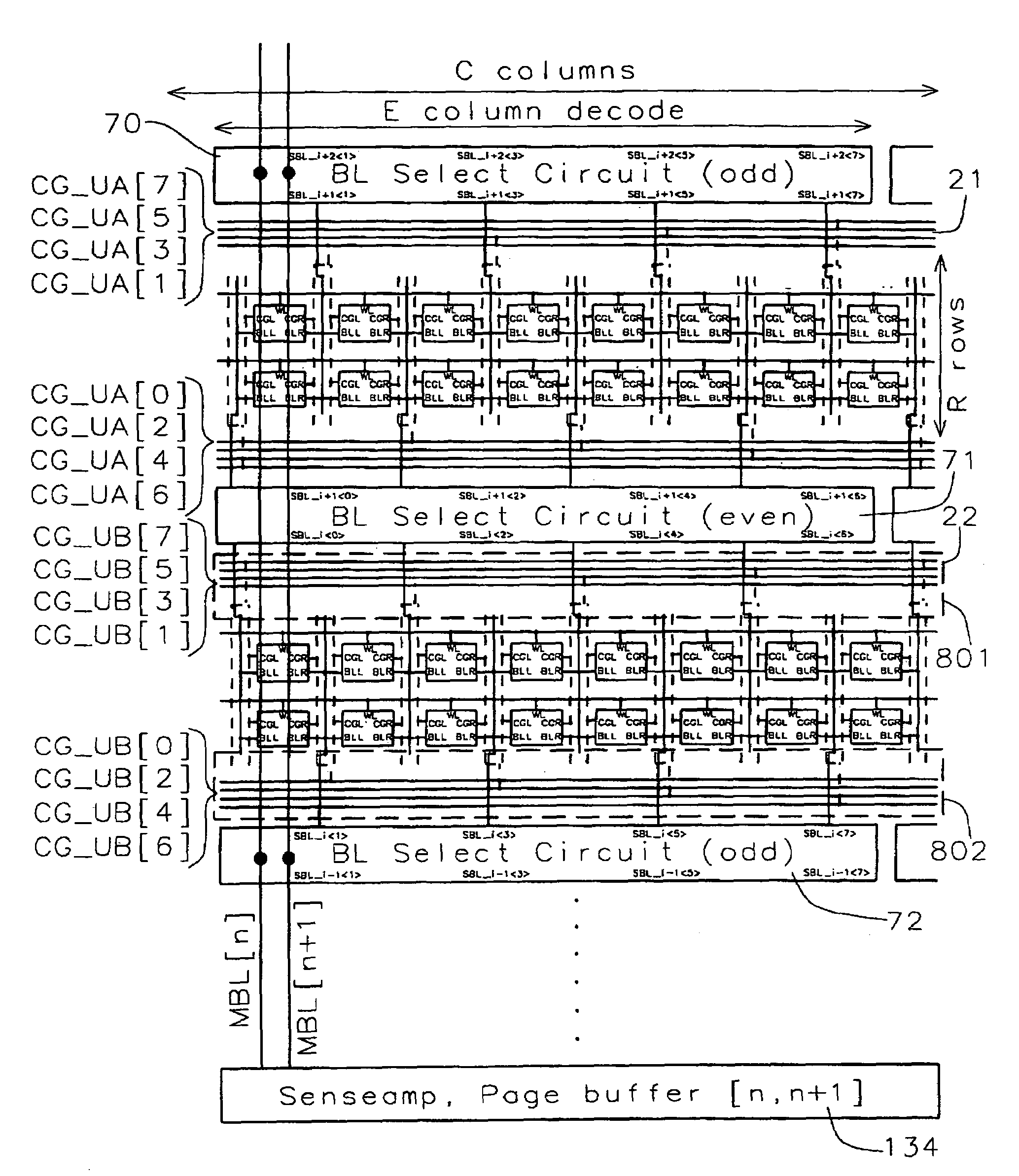
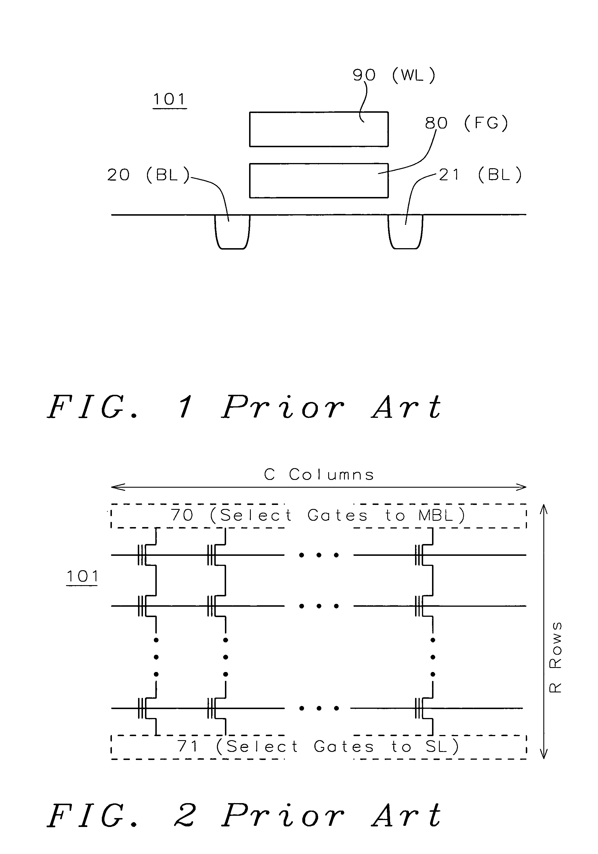
[0036]Array organization for Twin MONOS memory cells. In this invention, a new array organization is proposed. Unlike the array types described in the preceding Background section, cells that share the same word line do not necessarily share the same erase block. A schematic and block representation is given in FIG. 6. Twin MONOS cells are arranged in the diffusion bit array, with poly WL's running in a horizontal direction and diffusion BL's and poly CG's both running orthogonal to the WL's in a vertical direction.

[0037]In this figure, several memory units are shown which share a common sense amplifier / page buffer. Each UNIT's selected sub bit lines (SBL's) are connected via the UNIT's BL selection circuit to a global main bit line (MBL) which is connected to the sense amplifier / page buffer.

[0038]Two memory UNITS are shown in detail, UNIT A 21 and UNIT B 22. The number of rows in a single UNIT is R and the number of columns is C.

[0039]It is also possible to reduce the RC delay of t...

second embodiment

[0052]Depending on the metal pitch layout constraints, this method of CG segmentation may require an extra metal for the SBL. In the first array organization embodiment, the diffusion SBL is connected to the metal MBL in the sub-decode circuit. But in the second embodiment method, the diffusion SBL's may need to be connected to a metal SBL in the BL and CG stitch area. Then the metal SBL will be connected to the metal MBL in the sub-decode circuit.

[0053]As an alternative, the SBL and MBL may share the same metal layer by widening the cell pitch slightly.

[0054]Another alternative is shown in FIG. 13. The diffusion SBL of one segment could be connected through to the diffusion of the neighboring segment by either changing the order of CG and BL contacts (place the CG contacts closer to the memory array edge than the BL contact), or by creating a pass-through diffusion bridge 49.


PUM


Abstract

A non-volatile semiconductor storage device array organization for wide program operations is achieved. The device includes a memory cell array region in which a plurality of C columns and R rows of memory cells comprise one UNIT, arranged in a “diffusion bit” array organization which is comprised of R rows of word lines running in a first direction, and C columns of diffusion sub bit lines running in a second direction, and C columns of sub control gate lines running in the same second direction and a sense amplifier / page buffer area shared by several UNIT's through a bit decode circuit, wherein the diffusion sub bit lines in each of the UNIT's are connected to main bit lines which are in turn connected to the sense amplifier / page buffer area, wherein the bit decode circuit selects one diffusion sub bit line column of memory cells in every E columns.

Description

[0001]This application claims priority to U.S. Provisional Patent Application Ser. No. 60 / 569,388, filed on May 7, 2004, which is herein incorporated by reference in its entirety.BACKGROUND OF THE INVENTION[0002]1. Field of the Invention[0003]The present invention relates to semiconductor memory and in particular to the array organization for wide program operations and usage of non-volatile memory.[0004]2. Description of the Related Art[0005]Flash memory is characterized by having asymmetric program and erase units. Erase units, called ERASE BLOCKS, are typically large, on the order of 0.5 Mb or 1 Mb or higher. Program units are usually smaller and depend on the application demands. In NOR-type applications, only 16–32b are programmed at once. This data width historically has been limited by the high cell currents associated with the Channel Hot Electron (CHE) injection program method.[0006]Faster program by wide program data width is preferred for mass storage applications. Progra...

Claims


Application Information

Patent Timeline
Patent Type & Authority Patents(United States)
IPC IPC(8): G11C5/06G11C5/02G11C16/04G11C16/16G11C16/24H01L27/115
CPCG11C5/025G11C16/0475H01L27/115G11C16/24G11C16/16H10B69/00
Inventor OGURA, SEIKIOGURA, TOMOKOPARK, KI-TAEOGURA, NORISATOH, KIMIHIROSAITO, TOMOYA
Owner HALO LSI INC
Why Eureka
Try Eureka