Semiconductor memory device

a technology of memory device and semiconductor, which is applied in the direction of information storage, static storage, digital storage, etc., can solve the problems of increasing the capacity the reading/writing speed of a semiconductor memory device tends to be slower, and the length of the wiring in the device is becoming longer, so as to achieve the effect of reducing the sub-threshold current of the write buffer in the sub-amplifier circuit, reducing the standby current of power down and sel

Active Publication Date: 2007-03-20
LONGITUDE LICENSING LTD
View PDF15 Cites 7 Cited by
  • Summary
  • Abstract
  • Description
  • Claims
  • Application Information

AI Technical Summary

Benefits of technology

[0014]It is another object of the present invention to provide a semiconductor memory device that includes a metal mask for selecting, in accordance with type of the semiconductor memory device, e.g. DDR1 or DDR2, a circuit for reducing leak current from the sub-amplifiers.
[0015]It is another object of the present invention to provide a semiconductor memory device that can reduce leak current by controlling of a SCRC with a active command and a write command, selecting of a circuit in a SCRC, selecting of a substrate bias voltage, and so forth in combination.
[0016]According to one aspect of the present invention, in DRAM or the like having the specifications of DDR-2 and using a layered I / O system containing sub-amplifiers, a sub-threshold current reduction circuit (SCRC) controllable with a command is connected to sources of NMOS transistors which constitute a write buffer in the sub-amplifiers, in order to control the source potentials. The write buffer is used to reduce the potentials of the local I / O lines (LIO) to a low level at high speed.
[0029]In the standby state, the SCRC control signal controls the source potential of the NMOS transistor which constitutes the SCRC, so that the potential between the gate and the source is reduced. Thereby, the sub-threshold current for the write buffer in the sub-amplifier circuit can be reduced.
[0030]As a result, in the layered I / O system containing the sub-amplifiers, the standby currents in power down and self-refreshing can be reduced. Thus, both of the high speed processing and the reduction of the consumed power can be realized.

Problems solved by technology

Recently, capacity of a semiconductor memory device is becoming larger, and wiring length in the devices is becoming longer.
As a natural result, reading / writing speed to semiconductor memory devices tends to become slower.
On the other hand, according to a conventional semiconductor memory device, other kinds of problems have occurred.
Especially, it is intensively required to reduce power consumption of DRAMs.
Accordingly, this technique is not suitable for the case in which high-speed operation is required.

Method used


Image

  • Semiconductor memory device
  • Semiconductor memory device
  • Semiconductor memory device

Examples


first embodiment

[First Embodiment]

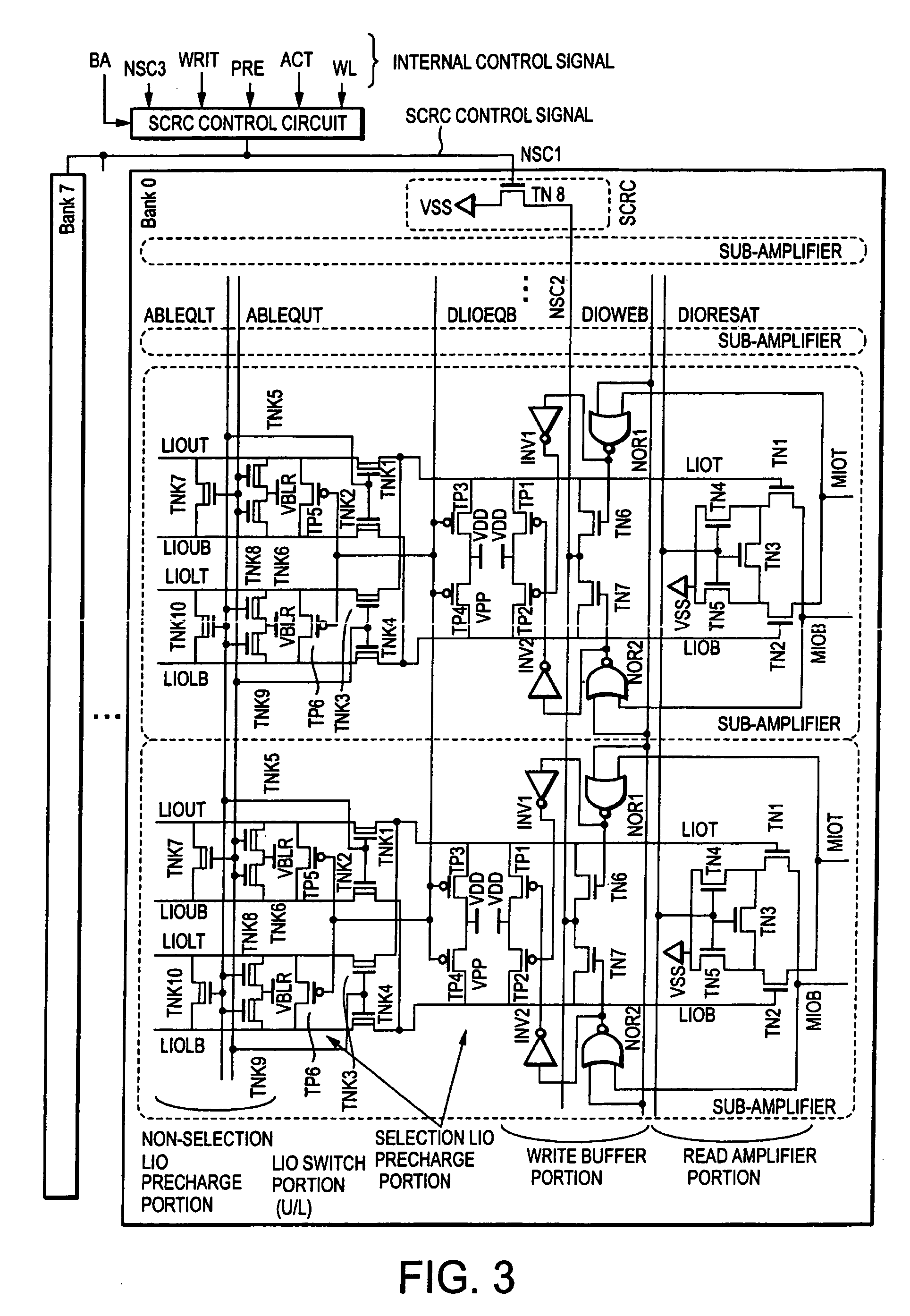
[0041]In this embodiment, the operation of a SCRC is controlled by a write command, and the SCRC is applied to write buffers of sub-amplifiers.

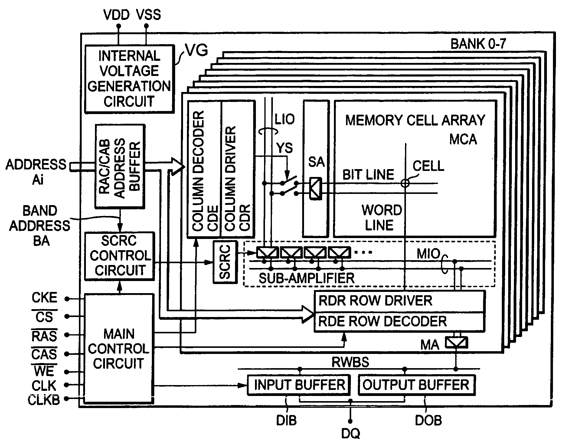
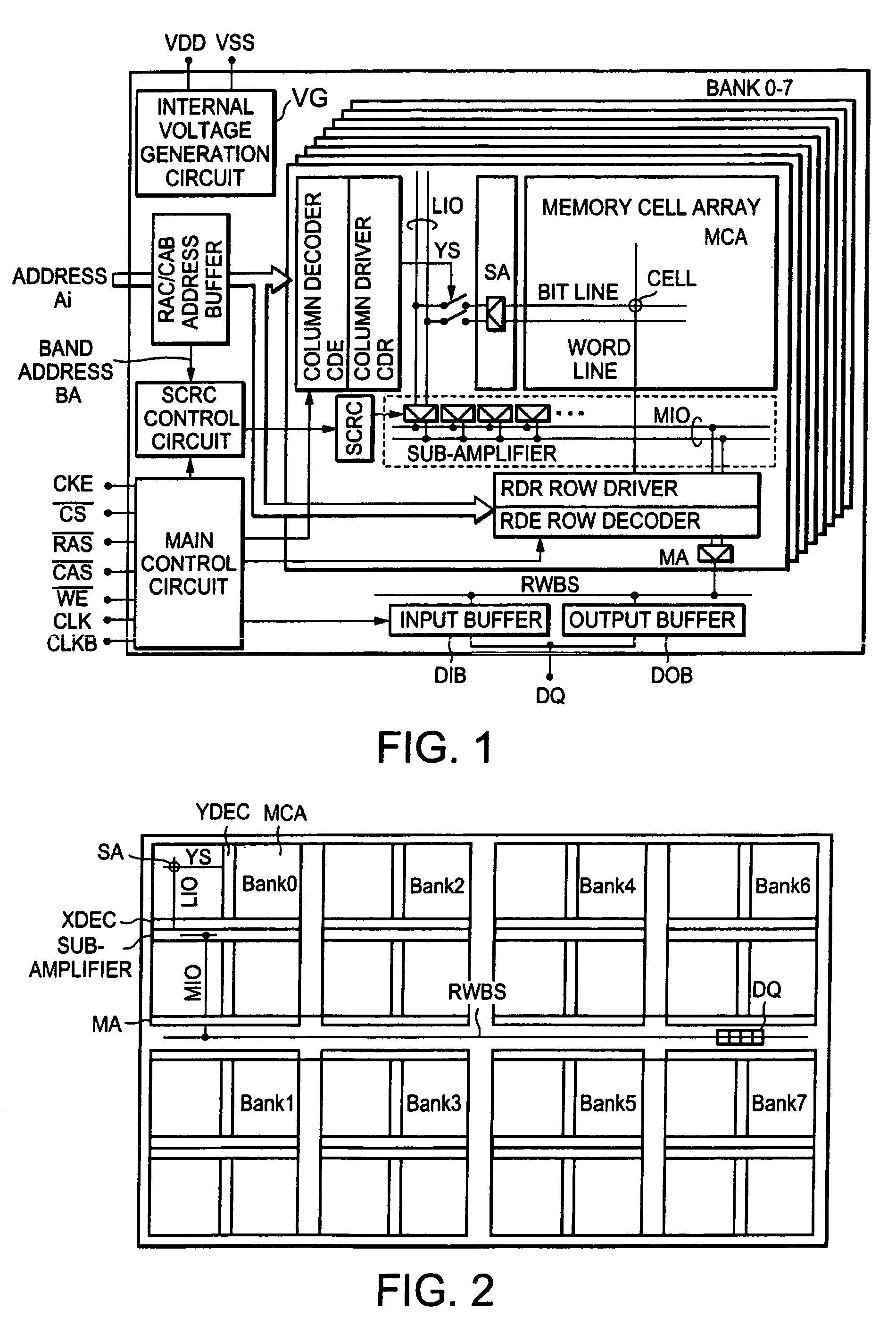
[0042]The outline of the configuration of a semiconductor memory device according to this embodiment is described with reference to FIG. 1. Specifically, the semiconductor memory device may be a 1 Gbit DDR-2 SDRAM. The semiconductor memory device includes a memory cell array MCA composed of a plurality of memory cells, address buffers (row address buffer and column address buffer) for designating an address in the memory cell array MCA, a row decoder RDE, a column decoder CDE, a row driver RDR, a column driver CDR, a sense amplifier SA for carrying out the read-write of data, a main amplifier MA, an output buffer DOB, an input buffer DIB, an input buffer DIB to which respective control signals are input, a main control circuit for generating an internal control signal, known units such as an internal voltage generating circu...

second embodiment

[Second Embodiment]

[0085]A second embodiment of the present invention will be described with reference to FIG. 6. The basic constitution is the same as that of the first embodiment. In the DDR-1 / DDR-2 combined-mounted DRAM, the SCRC configuration is further devised so as to be suitable for the DDR-1 specifications.

[0086]According to the DDR-1 specifications, the write latency WL is fixed at WL=1. Thus, in contrast to the first embodiment, the duration required to return the source potential of the transistors TN6 and TN7 in the write buffer portion to the ground potential can not be assured by setting the write latency at a long duration as in the first embodiment. Therefore, it is necessary to return the source potential to the ground potential earlier.

[0087]Therefore, according to this embodiment, in the case of coping with the DRAM having the specifications of DDR-1, the SCRC operation can be carried out with transistors having larger current supplying capabilities, specifically,...


PUM


Abstract

When a command is input to a semiconductor memory device, a sub-threshold current is reduced to a predetermined value corresponding to the command. After the reduction of the sub-threshold current is completed, the semiconductor memory device starts to operate corresponding to the command.

Description

BACKGROUND OF THE INVENTION[0001]1. Field of the Invention[0002]The present invention relates to reduction of power consumption by a semiconductor memory device and in particular to that by a semiconductor memory device in which a layered I / O system is installed.[0003]2. Description of the Related Art[0004]Recently, capacity of a semiconductor memory device is becoming larger, and wiring length in the devices is becoming longer. As a natural result, reading / writing speed to semiconductor memory devices tends to become slower. The layered I / O system is one of the techniques for improving the reading / writing speed.[0005]According to the layered I / O system, a sub-amplifier is arranged on an I / O line connecting between a main amplifier and a sense amplifier in order to compensate the potential of the I / O line and consequently to prevent reduction of the reading / writing speed.[0006]On the other hand, according to a conventional semiconductor memory device, other kinds of problems have oc...

Claims


Application Information

Patent Timeline
Patent Type & Authority Patents(United States)
IPC IPC(8): G11C7/02G11C11/06G11C7/10G11C8/00G11C11/409G11C11/4074G11C11/4097
CPCG11C7/1078G11C7/1096G11C11/4097G11C11/4074G11C2207/2227
Inventor MOCHIDA, NORIAKI
Owner LONGITUDE LICENSING LTD
Why Eureka
Try Eureka