Integrated photonic crystal structure and method of producing same

a photonic crystal and integrated technology, applied in the field of photonic crystals, can solve the problems of serious inability to introduce unwanted defects into three-dimensional photonic crystals during processing, and inability to achieve the effects of reducing the energy loss of the resonant cavity or waveguide structure, increasing the band gap, and effective reflecting, transmitting or confining electromagnetic waves

Inactive Publication Date: 2007-03-20
IGNIS PHOTONYX AS
View PDF15 Cites 35 Cited by
  • Summary
  • Abstract
  • Description
  • Claims
  • Application Information

AI Technical Summary

Benefits of technology

[0014]It is an object of the present invention to provide a new technique for producing three-dimensional photonic crystal structures for effectively reflecting, transmitting, filtering or confining electromagnetic waves, e.g. light. It is a further object to provide a relatively simple method that offers design flexibility and is suited for use in connection with integrated optical components. It is a further object of the present invention to provide a method that is suited for generating substantially planar (possibly corrugated) photonic crystal structures comprising layers having a non-mono-crystalline atomic structure. It is a further object of the present invention to provide a method of increasing the band gaps and allowing large multidimensional band gaps for one or all of the main polarisation states, enabling higher omni-directional reflectivity.
[0015]It is a further object of the present invention to provide an integrated photonic crystal structure with a large index contrast that is relatively simple to fabricate and to integrate in the normal production of an optical component.

Problems solved by technology

These types of photonic crystals, if designed for infrared or optical light, are difficult to fabricate, since the spatial periods must be comparable to the wavelength of operation.
However, the introduction of wanted defects into three-dimensional photonic crystals without introducing unwanted defects during processing is difficult.
These unwanted defects give rise to serious energy losses for the resonant cavity or waveguide structures.
However, the greatest problem and technological challenge in connection with the manufacture of photonic crystals concern the formation of a true three-dimensional structure in an industrial process scale.
However, the use of total internal reflection will only enable partial polarisation dependent band gaps, i.e. band gaps for certain discrete directions of propagation for narrow frequency ranges and only for one of the main polarisation states.
This will lead to substantial radiation loss in waveguides, waveguide bends, cavities and defects.
This structure yields a channel waveguide but is a two-dimensional PBG waveguide with a high index confinement in the third dimension that will not allow for a complete tuning of the characteristics of e.g. both polarisation states nor avoid radiation losses.
One disadvantage of this is that the realization of this structure will involve advanced and complicated lithography, deposition techniques, and complex three-dimensional alignment for the formation of the individual photonic crystal structures.
Furthermore, the introduction of wanted line defects into this corrugated structure is not trivial either which renders this technique most useful for the creation of defect free photonic crystals without the possibility for efficient localisation of energy.
Furthermore, at least one fourth defect in the layered structure results in an electromagnetic mode localised in the vicinity of the fourth defect.

Method used


Image

  • Integrated photonic crystal structure and method of producing same
  • Integrated photonic crystal structure and method of producing same
  • Integrated photonic crystal structure and method of producing same

Examples


example 1

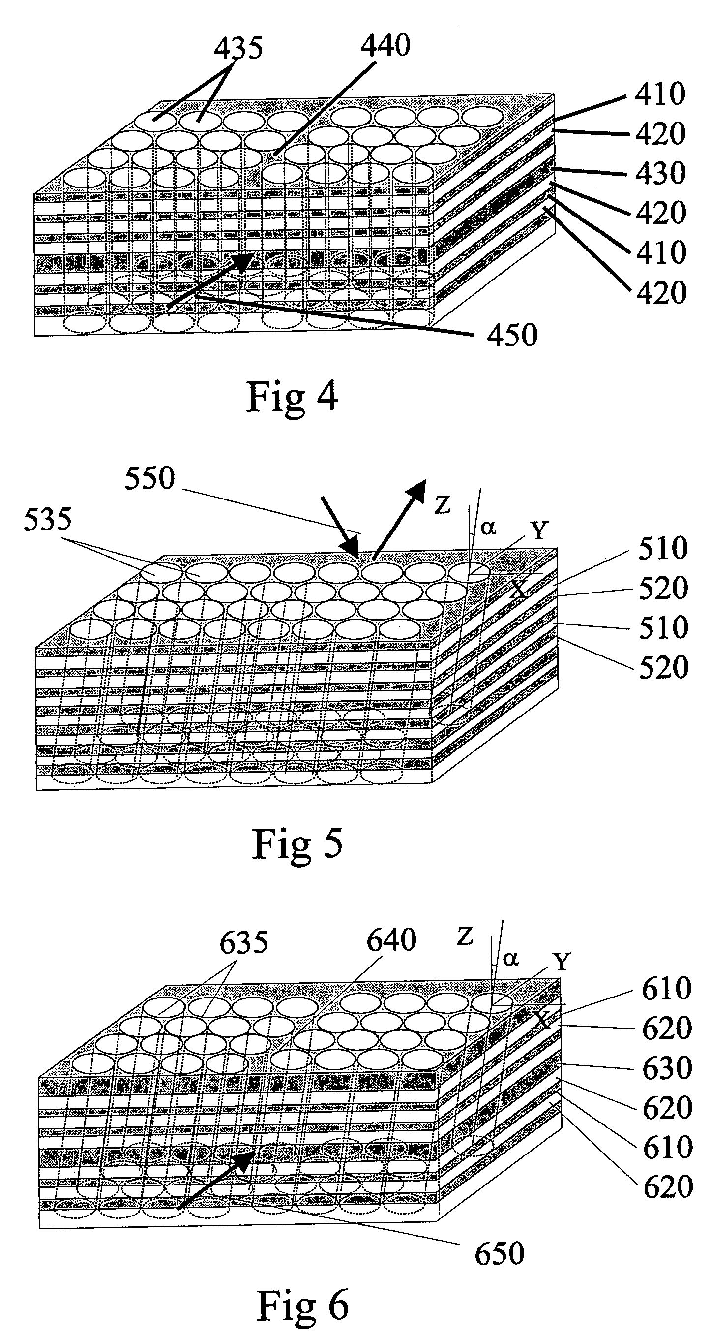
[0153]This example concerns an aspect of the present invention with α=1°. Said first surface is periodic and two-dimensional with the tangent plane (of said first surface) being a plane parallel to the (x, y) plane of a Cartesian coordinate system (x, y, z). Let a1=Λζ(√{square root over (3)} x+y) / 2 and a2=Λζ(√{square root over (3)} x−y) / 2 be two basis vectors that span the (x,y) plane characterising a two-dimensional triangular crystal lattice with lattice constant Λζ, and a3=Λzz be a third basis vector, x, y, and z being the Cartesian vectors of unit length.

[0154]Said first surface is defined as the set of points (x, y, z=S(ζ1, ζ2)) where S(ζ1, ζ2)=Aζ sin(2πζ1 / Λζ) sin(2πζ2 / Λζ)−ta / 2, where the coordinate pair (ζ1,ζ2) describes the (x,y) plane in the (a1, a2) coordinate system, Aζ is the amplitude of the modulation, Λζ is the period of modulation along a1 or a2, and where ta is the thickness of layer A of said first layered structure. The latter is made by depositing layer A with ref...

example 2

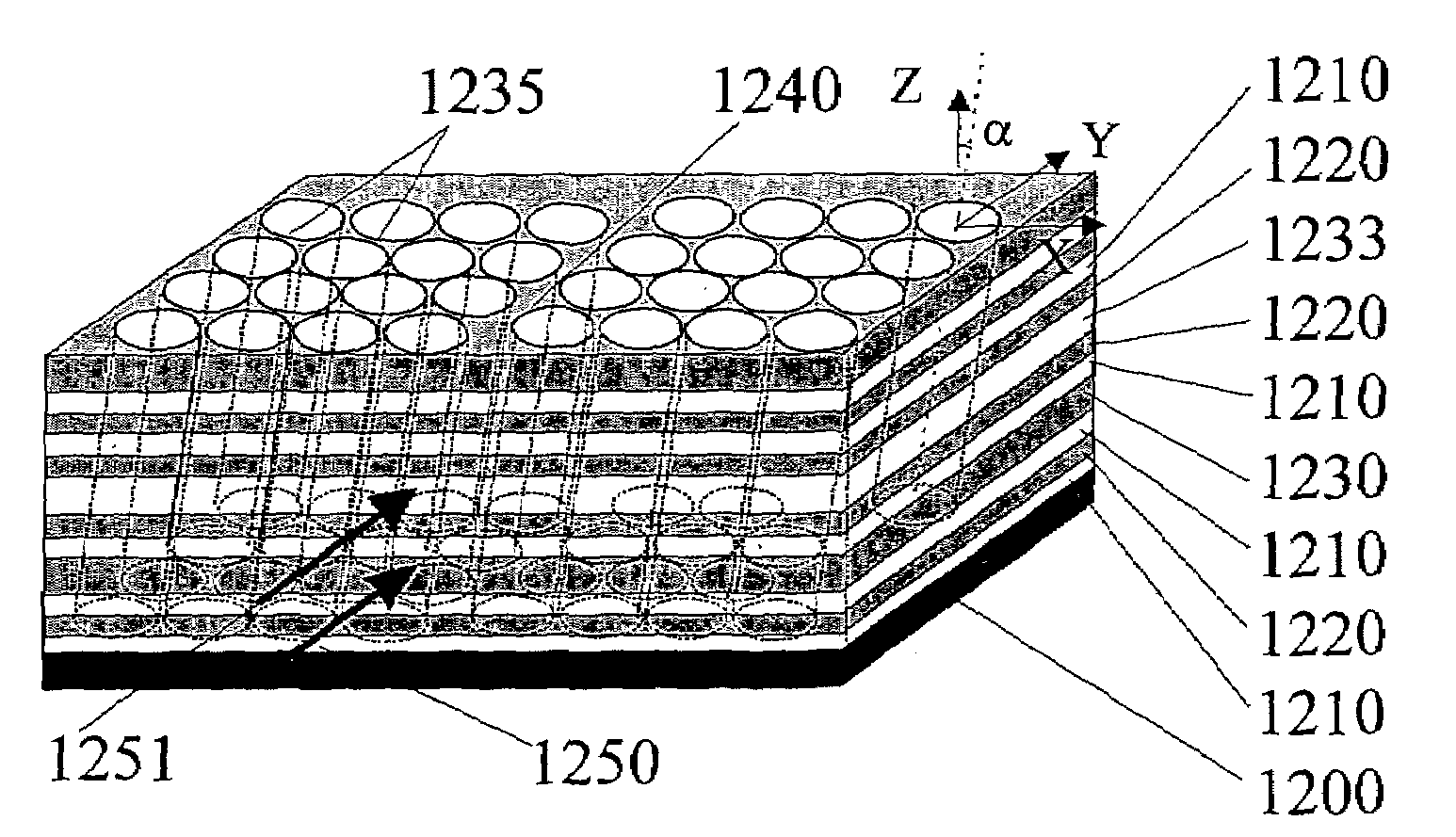
[0158]This example concerns an aspect of the present invention in the case where said first surface is planar and the intersecting angle of the second structure α=35.26°. In the following the (x,y) plane of a Cartesian coordinate system (x, y, z) is set parallel to the surface. A layered structure is formed by depositing layer A with refractive index na and thickness ta followed by layer B with refractive index nb and thickness tb in alternance. The period of this multilayer stack is Λz=ta+tb, which is the length of the unit of two layers that is repeated. In this example, the units are repeated an infinite number of times, but in reality approximately 10 to 20 units will be sufficient.

[0159]Let (x′, y′, z′) be a second Cartesian coordinate system where the z′-axis and the z-axis intersect at the angle α, and let a1=Λ(√{square root over (3)} x+y) / 2 and a2=Λ(√{square root over (3)} x−y) / 2 be two basis vectors that span the (x,y) plane characterising a two-dimensional triangular cryst...

example 3

[0163]This example concerns an aspect of the present invention in the case where the first surface is planar and the intersecting angle of the second structure α=0°. In the following the (x,y) plane of a Cartesian coordinate system (x, y, z) is set parallel to the surface. A layered structure is formed by depositing layer A with refractive index na and thickness ta followed by layer B with refractive index nb and thickness tb in alternance. The period of this multilayer stack is Λz=ta+tb, which is the length of the unit of two layers that is repeated. In this example, the units are repeated an infinite number of times, but in reality approximately 10 to 20 units will be sufficient.

[0164]Let (x′, y′, z′) be a second Cartesian coordinate system where the z′-axis and the z-axis intersect at an angle α, and let a1=Λ(√{square root over (3)} x+y) / 2 and a2=Λ(√{square root over (3)} x−y) / 2 be two basis vectors that span the (x,y) plane characterising a two-dimensional triangular crystal lat...


PUM


Abstract

An integrated photonic crystal (IPC) structure and method of producing the same in which the IPC structure includes a first layered sub-structure with a surface and a one-dimensional periodic refractive index variation along the direction perpendicular to the surface, and a second sub-structure with a plurality of essentially straight identical passages arranged in a two-dimensional periodic pattern cutting through the layered structure at an angle α. First and second defects in the first and second sub-structures, respectively, enable electromagnetic modes to be localized in the vicinity of the defects and allow photonic crystal waveguide to be constructed that can control and filter light very efficiently and minimize radiation losses.

Description

[0001]This is a nationalization of PCT / DK02 / 00700 filed Oct. 21, 2002 and published in English, which was entitled to and claimed the priority of two co-pending U.S. Provisional applications, Ser. No. 60 / 330,521 filed Oct. 24, 2001, and Ser. No. 60 / 387,892 filed Jun. 13, 2002.TECHNICAL FIELD OF THE INVENTION[0002]The invention relates to the field of photonic crystals. In particular, this invention relates to a photonic crystal structure for the transmission / reflection and filtering of electromagnetic waves. Further the invention relates to a photonic crystal structure wherein waveguide cores and / or reflectors are formed.[0003]The invention also concerns a method for the manufacture of integrated photonic crystal structures for the transmission / reflection and filtering of electromagnetic waves.DESCRIPTION OF RELATED ART[0004]In recent years periodic dielectric media, so called photonic crystals, have drawn a lot of interest in the research community, and many structures have been st...

Claims


Application Information

Patent Timeline
Patent Type & Authority Patents(United States)
IPC IPC(8): G02B6/10G02B6/12G02B6/122G02B6/13G02B6/132
CPCB82Y20/00G02B6/1225G02B6/132G02B6/13G02B2006/12176
Inventor DRIDI, KIM HAKIMMATTSSON, KENT ERIK
Owner IGNIS PHOTONYX AS
Why Eureka
Try Eureka