Wireless communication receiver

Inactive Publication Date: 2007-03-20
RENESAS ELECTRONICS CORP
View PDF19 Cites 13 Cited by
  • Summary
  • Abstract
  • Description
  • Claims
  • Application Information

AI Technical Summary

Benefits of technology

[0032]However, if metal oxide semiconductor field effect transistors (which will be referred to as “MOSFETs” hereinafter) are used as the above switches, the effect of on-resistance presents a problem and the gate width of the MOSFETs need to increase. If these large MOSFETs are used, due to their parasitic capacitance, gain rises at a high frequency band. This gain rise can be avoided by connecting the collectors of the differential pair of transistors via a capacitor. This can produce the same effect that a low-pass filter is connected to the output.
[0033]By comparison between the above-described programmable gain amplifier circuitry in which the emitters of the transistors forming one differential pair are connected via a plurality of resistors and the plurality of resistors are connected and disconnected by the associated switches and the conventional programmable gain amplifier circuitry in which the transistors of a plurality of differential pairs are individual

Problems solved by technology

In such receivers including the above programmable gain amplifiers, after the RF frequency of received signals is downconverted to a baseband by d

Method used


Image

  • Wireless communication receiver
  • Wireless communication receiver
  • Wireless communication receiver

Examples


embodiment 2

[0127]A preferred Embodiment 2 of the present invention will be described, using FIG. 5. As another method of suppressing the effect of noise produced by gain change made by the programmable gain amplifiers by which gains are adjustable in steps, means for causing the programmable gain amplifiers to make gain change at random timing are applied. Gain change at random timing can eliminate the possibility that timing of receiving control signals such as TPC, TFCI, and Pilot always coincides with timing of noise occurring, that is, when the programmable gain amplifiers make gain change.

[0128]Because of the random mode of gain change, the sequencer need not identify which slot format is being received. For example, a device that randomly delays the control signals to the programmable gain amplifiers should be installed in the receiver circuitry. As an example of such device, a device configured as shown in FIG. 5 should be installed on the control signal line. Specifically, in the recei...

embodiment 3

[0130]A preferred Embodiment 3 of the present invention will be described, using FIG. 9. In a multistage configuration with programmable gain amplifiers by which gains are adjustable in steps, gain change made by the first-stage programmable gain amplifier results in a great noise. This is because noise produced in the first stage is amplified by the following stages of programmable gain amplifiers.

[0131]In this embodiment, the first-stage programmable gain amplifier is arranged to have hysteresis. This can reduce both the frequency of gain change by the first-stage programmable gain amplifier and the frequency of a great noise occurring. For example, when a programmable gain amplifiers section is composed of three stages of programmable gain amplifiers, PGA1, PGA2, and PGA3, as is shown in FIG. 9A, a gain table should be created so that PGA1 has hysteresis, as is shown in FIG. 9B. In FIG. 9B, the receiving level Ior on the abscissa decreases toward the right and gain on the ordinat...

embodiment 4

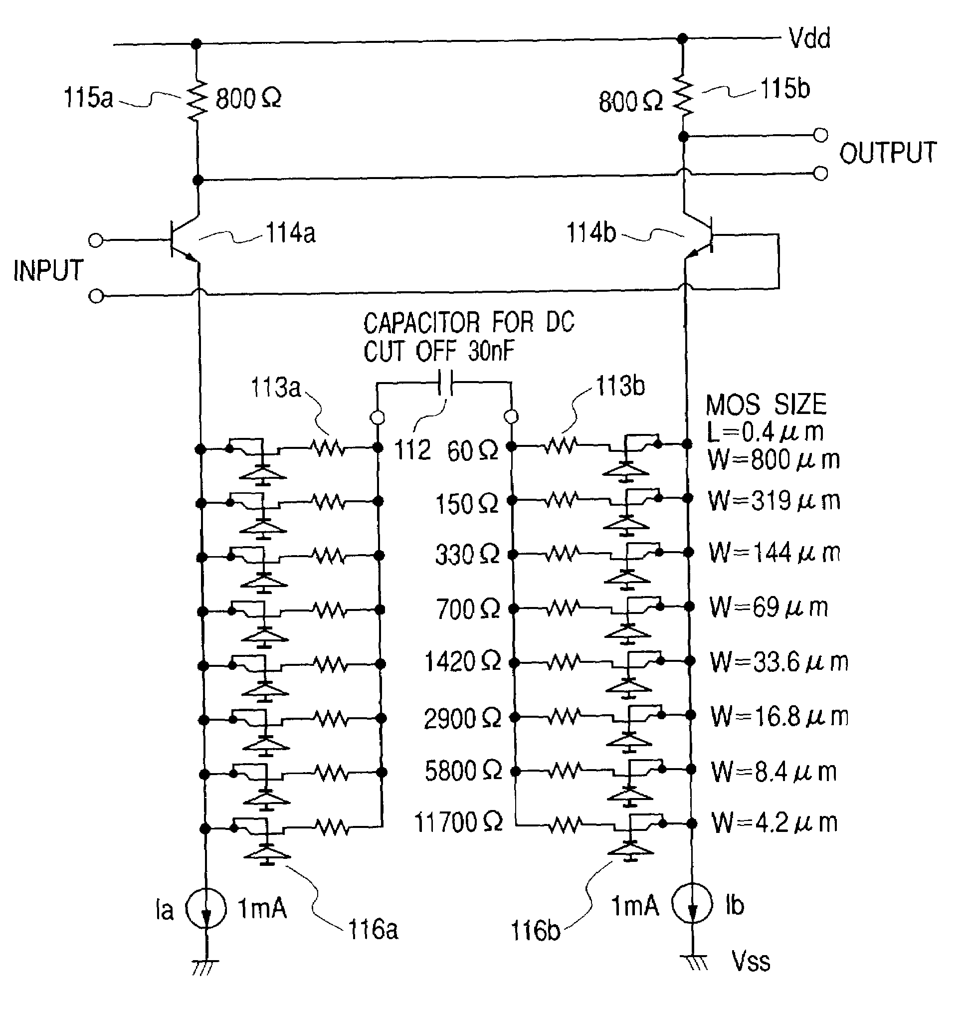
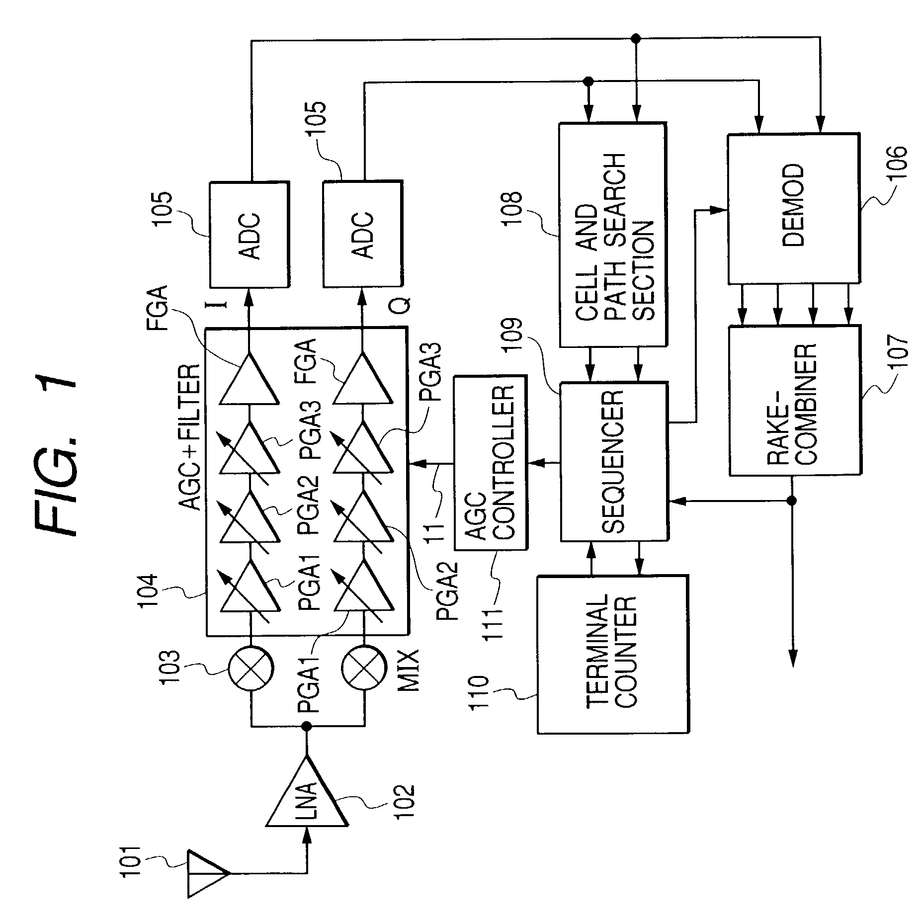
[0132]A preferred Embodiment 4 of the present invention will be described, using FIG. 28. FIG. 28 is a circuitry diagram showing a configuration example of the first-stage programmable gain amplifier out of the three programmable gain PGA1 to PGA3 by which gains are adjustable in steps in the programmable gain amplifiers and filters section 104 in the receiver circuitry of FIG. 1. In the circuitry of FIG. 28, the capacitor can perform the high-pass filter function as well.

[0133]The programmable gain amplifier by which gains are adjustable in steps, shown in FIG. 28, is a circuit arranged so noise accompanying gain change is hard to produce. In the programmable gain amplifier by which gains are adjustable in steps, shown in FIG. 28, reference numeral 112 denotes the capacitor. One end of the capacitor 112 is connected via a plurality of parallel resistors 113a and switches 116a which are respectively connected in series to the resistors 113a to the emitter of a transistor 114a. Simil...


PUM


Abstract

A wireless communication receiver that is able to lessen the effect of noise that accompanies gain change by programmable gain amplifiers. The receiver includes an AGC controller which controls the timing at which the programmable gain amplifiers make gain change, using a terminal counter and a sequencer. The receiver prevents gain change noise signals during the reception of control signals and other signals that are susceptible to noise. By the timing control feature, the programmable gain amplifiers make gain change while reducing noise impact.

Description

BACKGROUND OF THE INVENTION[0001]1. Field of the Invention[0002]The present invention relates to a wireless communication receiver (which will be simply referred to as a “receiver” hereinafter) and, more particularly, to a direct conversion type receiver using programmable gain amplifiers by which gains are adjustable in steps and being able to suppress the effect of noise that accompanies gain change by the programmable gain amplifiers.[0003]2. Description of the Related Art[0004]One type of signals to be received by receivers for Wideband Code Division Multiple Access (W-CDMA), standardization of which is pursued by the 3rd Generation Partnership Project (3GPP), Dedicated Physical Channel signals (which will be referred to as DPCH signals hereinafter) are formatted in a recommended format which is shown in FIG. 2A.[0005]The DPCH signals are transmitted and received in frames, each frame being 10 msec., and one frame is divided into 15 slots, each slot being 666 μsec. One slot cont...

Claims


Application Information

Patent Timeline
IPC IPC(8): H04B1/06H03G3/20H03G3/30H04B1/10
CPCH03G3/3052H03G3/3078H04B1/707
Inventor AKAMINE, YUKINORIKAJIWARA, HISAYOSHITANAKA, SATOSHIYANO, TAKASHIISHII, HIROTAKEYAMAMOTO, AKIOHORI, KAZUAKIHIKASA, KAZUHIKO
Owner RENESAS ELECTRONICS CORP
Why Eureka
Try Eureka