Antenna module

a technology of antenna module and antenna module, which is applied in the direction of loop antennas with ferromagnetic cores, non-resonant long antennas, protective materials radiating elements, etc., can solve the problems of large antenna module size, large antenna module and electronic instrument incorporating antenna modules, and large antenna module size. , to achieve the effect of reducing the mounting area necessary, increasing the overall capacitance value, and increasing the broadband

Inactive Publication Date: 2007-04-03
PANASONIC CORP
View PDF46 Cites 5 Cited by
  • Summary
  • Abstract
  • Description
  • Claims
  • Application Information

AI Technical Summary

Benefits of technology

[0011]The invention arranges the capacitive conductor in opposition to the helical part provided on the substrate, thereby enabling to generate a capacitive component parallel to a capacity existing in the substrate. Further, it is possible to easily increase an overall capacitive value owing to the parallel capacitive component, and to progress the broadband.
[0012]Since the capacitive conductor exists on a bottom of the chip antenna when mounting the chip antenna, the capacitive conductor is more efficient than providing a large additional conductor at the lead end of the chip antenna, not requiring an excessive mounting area. That is, an effect of making the broadband is further increased, curtailing the mounting area necessary as a whole. In short, it is possible to make efficient use of a wasteful area created when mounting the chip antenna but not used to mounting of other parts, and to increase the capacitive component for realizing the broadband. The antenna is not therefore made large sized but can be maintained to be small sized.
[0013]Further, it is possible to realize multiple resonances when connecting a plurality of chip antennas, and make the broadband by the efficient mounting area.
[0015]With such a small sized broadband antenna module, the electronic instrument incorporated there with can be much reduced in dimension.

Problems solved by technology

However, when providing the additional conductor at the lead end of the pattern antenna as the meander antenna, there has been a problem that the antenna module is large scaled, because the pattern antenna itself requires a large area.
In particular, for further advancing the broadband, the load capacity at the lead end of the antenna must be made large sized, but if being too large sized, the area at the lead end of the antenna becomes accordingly large sized, so that a problem occurs that the antenna module and the electronic instrument incorporating the antenna module are very much oversized.
Further, being too large sized, a balance cannot be kept with an effect of making broadband, and efficiency is not sufficiently brought about in comparison with the large scale.

Method used


Image

  • Antenna module
  • Antenna module
  • Antenna module

Examples


embodiment 1

(Embodiment 1)

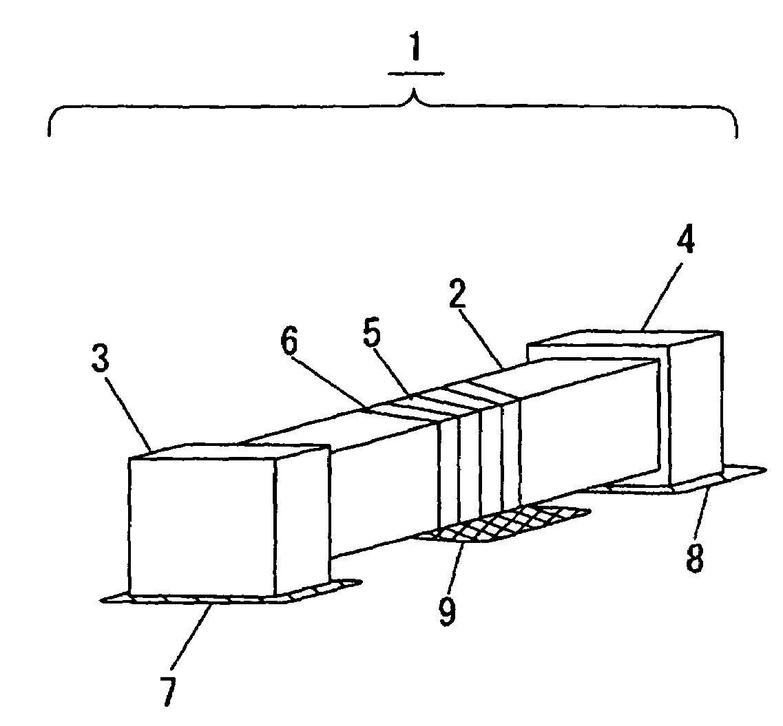
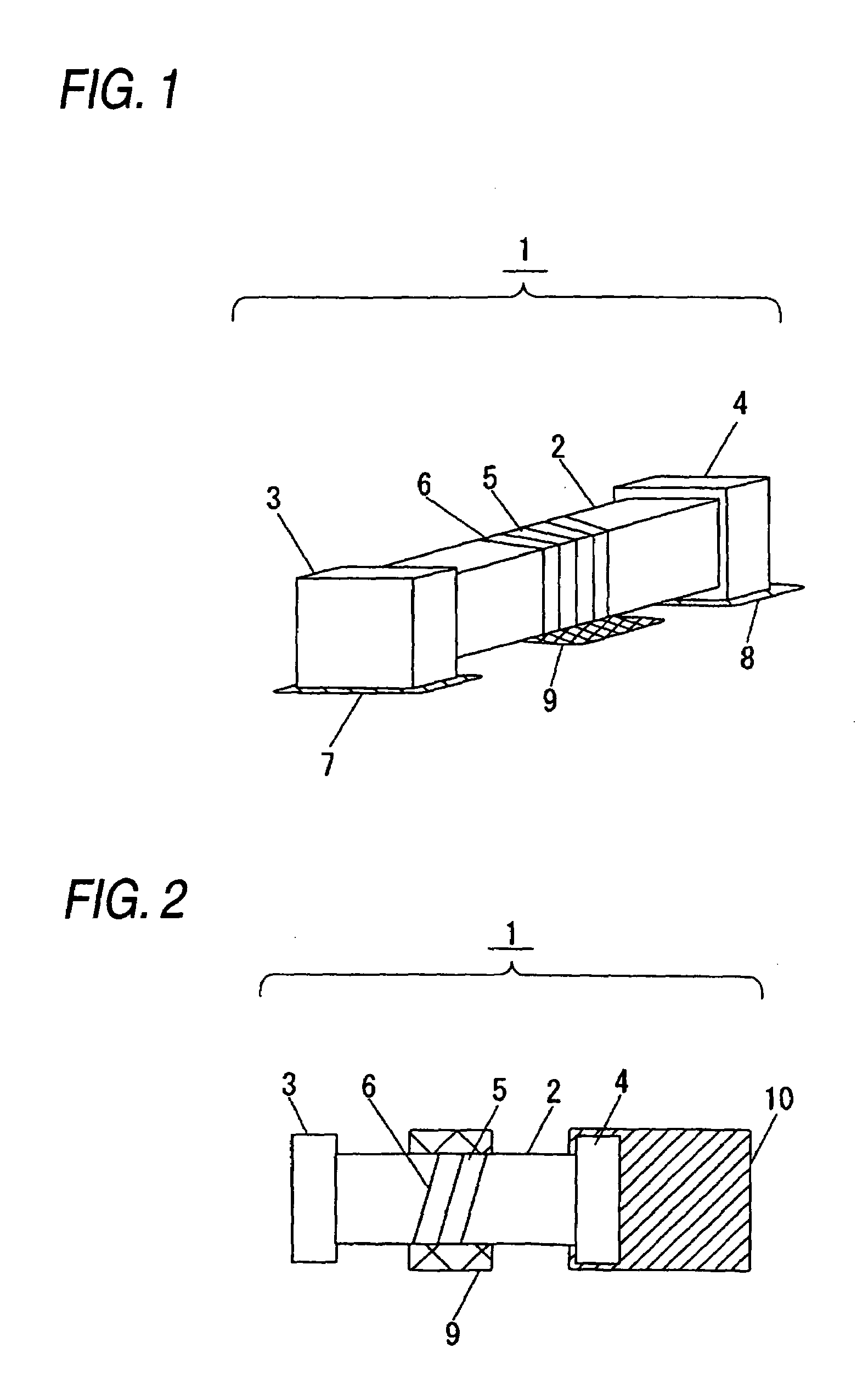
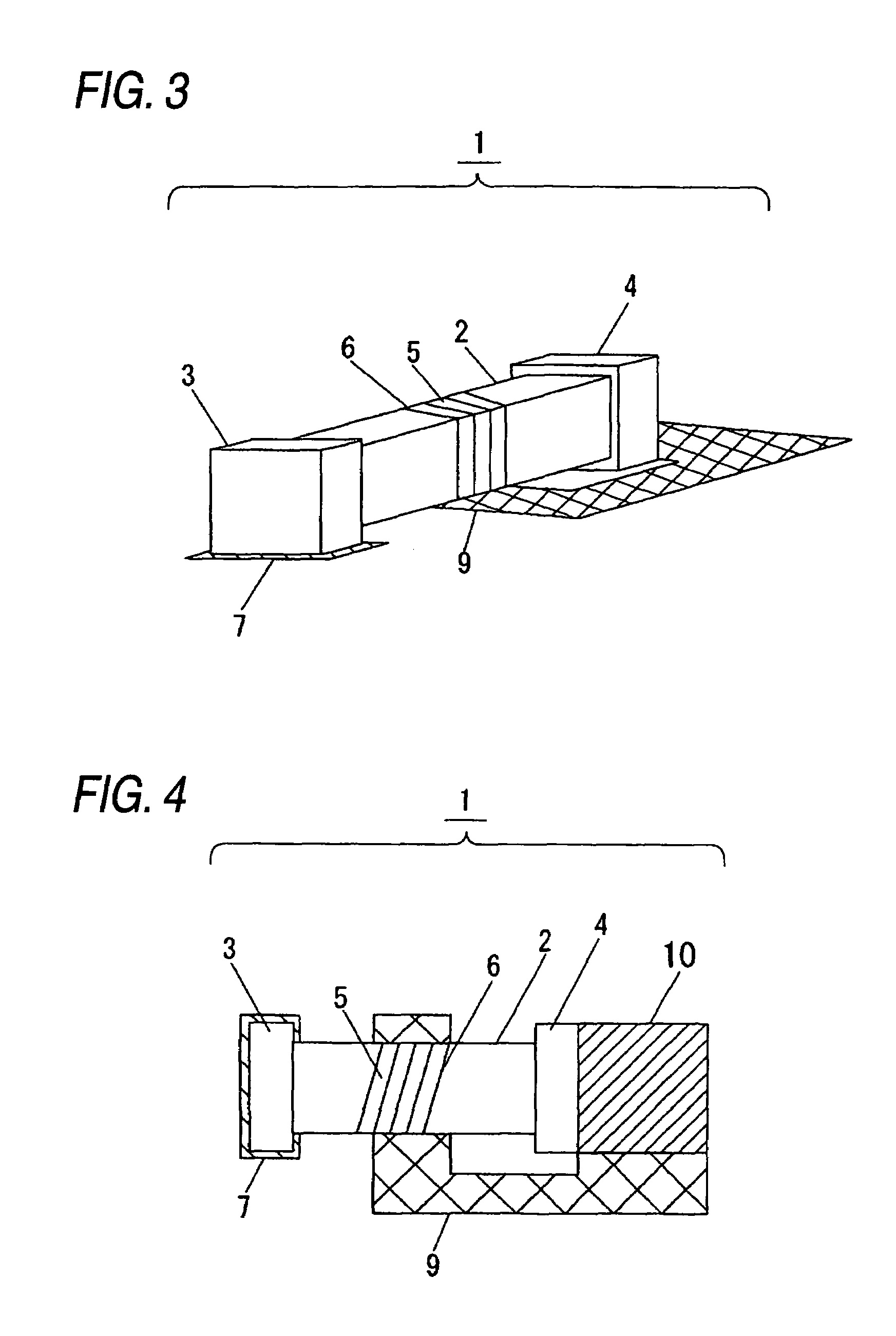
[0039]FIG. 1 and FIG. 3 are perspective views of the antenna module in the embodiment 1 of the invention, and FIG. 2, FIG. 4 and FIG. 7 are structural views of the antenna module in the embodiment 1 of the invention. FIG. 5 is an equivalent circuit diagram of the antenna module shown in FIG. 3. FIG. 8 is the equivalent circuit diagram of the antenna module shown in FIG. 7. FIG. 16 and FIG. 17 are perspective views of the other antenna modules in the embodiment 1 of the invention.

[0040]Numeral 1 designates the chip antenna, 2 designates the substrate, 3 and 4 are terminal parts, 5 is the helical part, 6 is spiral grooves, 7 is the feeding portion, 8 is the open portion, and 9 is the capacitive conductor. The mounting body mounting these members thereon is not shown.

[0041]The chip antenna 1 is composed in that the terminal parts 3, 4 are provided at both ends of the substrate 2, a helical part 5 is defined by forming a spiral grooves 6 formed in such a manner that a cond...

embodiment 2

(Embodiment 2)

[0088]In Embodiment 2, explanation will be made to the antenna module having a plurality of chip antennas. FIGS. 9, 10, 11, and 13 are the structures of the antenna module in Embodiment 2 of the invention. FIG. 12 is the equivalent circuit diagram of one part of the antenna module shown in FIG. 9.

[0089]FIGS. 9, 10 and 11 show the structures connected in series with the two chip antennas. Numerals 11 designates the connected conductor and 12 is the antenna module. The connected conductor 11 connects in series the two chip antennas. This connected conductor is formed with the mounted land, the soldered face or the metal film, and if the width direction is made not largely exceed the width direction of the chip antenna 1, the antenna module is miniaturized. The same is applied to the capacitive conductor. The signal current is sent to the chip antenna 1 via the feeding portion 7, and since the chip antenna 1 is connected in series via the connected conductor 11, the signa...

embodiment 3

(Embodiment 3)

[0107]FIG. 14 is a structural view of the electronic instrument in the embodiment 3 of the invention. The electronic instrument shown in FIG. 14 is the notebook personal computer, portable terminal, and portable telephone, and they are incorporated with the antenna module mounted with the chip antenna discussed in Embodiments 1 and 2.

[0108]Numeral 30 designates the case, 32 designates the high frequency circuit, 33 is a processing circuit, 34 is a control circuit, and 35 is an electric power source.

[0109]The case 30 is, for example, a case of the portable telephone, or of the notebook personal computer, and the case 30 may contain a display, a memory, a hard disc or an external storage medium.

[0110]The high frequency circuit applies high frequency signal current to the antenna module 31, or receives the high frequency signal received at the antenna module 31 and detects waves. The high frequency circuit contains a power amplifier necessary to signal transmission, a low...


PUM


Abstract

The invention is to provide such an antenna module making broadband of transmitting and receiving frequencies, while realizing miniaturization. The invention has a structure comprising a mounting body; a chip antenna having a substrate mounted on the mounting body and a substrate and a couple of terminal parts provided on the substrate; an feeding portion to which one of the terminal parts provided on the mounting body is connected; a open portion to which the other of the terminal parts provided on the mounting body is connected; and a capacitive conductor provided in opposition to the substrate, thereby to make use of a bottom area hidden when mounting the chip antenna so as to increase capacitive components for realizing broadband of the antenna module.

Description

BACKGROUND OF THE INVENTION[0001]The present invention relates to an antenna module suitably used to electronic instruments performing wireless communications such as mobile communications or personal computers.[0002]There have recently been more portable terminals mounted with antenna modules provided for performing wireless data communications to other electronic instruments in addition to whip antennas or built-in antennas provided for voice communication.[0003]Besides, there have also been increased portable mobile electronic instruments such as notebook personal computers, using wireless LAN for performing wireless data communications; therefore, many of the electronic instruments have the antenna modules therein.[0004]Further, in the recent portable telephones or notebook personal computers, miniaturization and low consumption of electric power are indispensable requirements, and an antenna device has been demanded to reduce its dimension. In addition, with increase of transmi...

Claims


Application Information

Patent Timeline
Patent Type & Authority Patents(United States)
IPC IPC(8): H01Q1/24H01Q1/40H01Q1/36H01Q5/10H01Q7/08H01Q11/08H04B1/38
CPCH01Q1/243H01Q1/362H01Q7/08H01Q11/08H01Q1/24H01Q23/00H04B1/38
Inventor NOGUCHI, TOSHIHARUFUJIMURA, MUNENORITOKUNAGA, HIROMIMARUYAMA, KEISUKEMIZOGUCHI, YOSHITAKA
Owner PANASONIC CORP
Why Eureka
Try Eureka