Semiconductor device, and display device and electronic device utilizing the same

a technology of semiconductor devices and electronic devices, applied in the direction of identification means, pulse techniques, instruments, etc., can solve the problems of reducing size and weight, and it is difficult to reduce manufacturing costs to the level sufficiently low, so as to reduce manufacturing costs, prevent the amplitude of output signals from being decreased, and reduce the effect of amplitud

Active Publication Date: 2007-04-10
SEMICON ENERGY LAB CO LTD
View PDF68 Cites 136 Cited by
  • Summary
  • Abstract
  • Description
  • Claims
  • Application Information

AI Technical Summary

Benefits of technology

[0048]According to the configuration of the invention, either terminal of a capacitor configuring a bootstrap circuit is easily brought into a floating state. As a result, the amplitude of an output signal is prevented from being decreased. In addition, even when the amplitude of an input signal is small, ei

Problems solved by technology

As mobile electronic devices are reduced in size and weight, demand for a display device using a self-light emitting element and a liquid crystal element and the like such as an organic EL element, an FED (Field Emission Display), and an element used for a liquid crystal display is rapidly increasing; however

Method used


Image

  • Semiconductor device, and display device and electronic device utilizing the same
  • Semiconductor device, and display device and electronic device utilizing the same
  • Semiconductor device, and display device and electronic device utilizing the same

Examples


embodiment

[0122][Embodiment Mode 3]

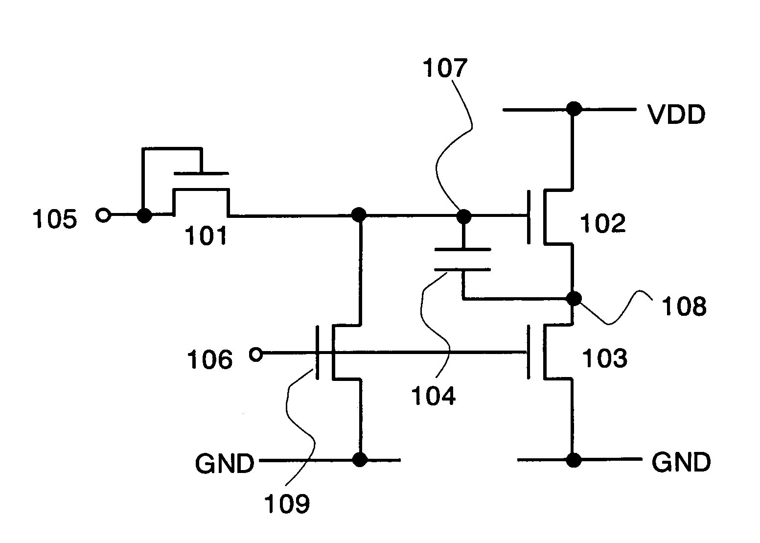
[0123]Described in this embodiment mode is the inverter circuit for dealing with the first and second problems described in the section of the problems to be solved by the invention, which is obtained by modifying the circuit described in Embodiment Mode 1. In this embodiment mode, an inverter circuit for dealing with the first problem is described by modifying the circuit in FIG. 34.

[0124]FIG. 8 shows a modified inverter circuit of FIG. 34. A diode-connected transistor 801 is connected in series to a transistor 3409. It is to be noted that although the transistor 801 is disposed between the drain terminal of the transistor 3409 and the terminal 3407, the invention is not limited to this. For example, it may be connected to the source terminal side of the transistor 3409.

[0125]As described above, by disposing the transistor 801, the potential at the terminal 3407 is prevented from dropping to a large degree. Therefore, the potential at the terminal 3407 is i...

embodiment 1

[0191][Embodiment 1]

[0192]Described in this embodiment is the configuration and operation of a display device, a signal line driver circuit and the like. The circuit configurations described in Embodiment Modes 1 to 5 can be applied to a part of a signal line driver circuit or a part of a gate line driver circuit.

[0193]Referring to FIG. 28, a display device includes pixels 2801, a gate line driver circuit 2802 and a signal line driver circuit 2810. The gate line driver circuit 2802 sequentially outputs selection signals to the pixels 2801 and the signal line driver circuit 2810 sequentially outputs video signals to the pixels 2801. In the pixels 2801, an image is displayed by controlling the state of light according to the video signals. Voltage is frequently employed as a video signal input from the signal line driver circuit 2810 to the pixels 2801. That is, the states of a display element disposed in the pixel and an element for controlling the display element are changed accordi...

embodiment 2

[0214][Embodiment 2]

[0215]Electronic devices, using the semiconductor device of the invention, include a video camera, a digital camera, a goggle type display (head mounted display), a navigation system, a sound reproducing device (a car audio equipment, an audio component stereo and the like), a laptop personal computer, a game machine, a portable information terminal (a mobile computer, a cellular phone, a portable game machine, an electronic book and the like), an image reproducing device including a recording medium (more specifically, an apparatus which can reproduce a recording medium such as a digital versatile disc (DVD) and so forth, and includes a display for displaying the reproduced image) or the like. Specific examples of these electronic devices are shown in FIGS. 32.

[0216]FIG. 32A shows a light emitting device, which includes a housing 13001, a support base 13002, a display portion 13003, a speaker portion 13004, a video input terminal 13005 and the like. The display ...


PUM


Abstract

A semiconductor device having a normal function means is provided, in which the amplitude of an output signal is prevented from being decreased even when a digital circuit using transistors having one conductivity is employed. By turning OFF a diode-connected transistor 101, the gate terminal of a first transistor 102 is brought into a floating state. At this time, the first transistor 102 is ON and its gate-source voltage is stored in a capacitor. Then, when a potential at the source terminal of the first transistor 102 is increased, a potential at the gate terminal of the first transistor 102 is increased as well by bootstrap effect. As a result, the amplitude of an output signal is prevented from being decreased.

Description

INDUSTRIAL FIELD FOR THE INVENTION[0001]The present invention relates to a configuration of a digital circuit. More particularly, the invention relates to a technology for amplifying an output signal even larger by using a bootstrap circuit, and further to a display device, a semiconductor device or an electronic device each using the technology.BACKGROUND ART[0002]In recent years, display devices in which a semiconductor thin film is formed on an insulator such as a glass substrate, in particular active matrix display devices using thin film transistors (hereinafter referred to as TFTs), have been in widespread use in various fields. An active matrix display device using TFTs has several hundred thousand to several million pixels arranged in matrix, and it displays images by controlling the electric charge in each pixel by using a TFT disposed in each pixel.[0003]As a recent technology, the technology relating to poly-silicon TFTs in which a driver circuit is simultaneously formed ...

Claims


Application Information

Patent Timeline
IPC IPC(8): G09G5/00G09F9/30H03K3/356G09G3/00G09G3/20H01L21/8238H03F3/16H03K17/00H03K17/06H03K17/687H03K19/094H03K19/096
CPCH01L27/1255H01L27/124G09G3/36H03K19/018507G09G2310/0267G09G2310/0275G09G5/003G09G3/20G09G2310/0286G09G2310/0291G09G2310/0289G09G2330/021
Inventor KIMURA, HAJIMESHIONOIRI, YUTAKA
Owner SEMICON ENERGY LAB CO LTD
Why Eureka
Try Eureka