Semiconductor light emitting device, its manufacturing method, integrated semiconductor light emitting apparatus, its manufacturing method, illuminating apparatus, and its manufacturing method

a technology of semiconductor light emitting device, which is applied in the direction of semiconductor devices, electrical devices, basic electric elements, etc., can solve the problems of complicated steps and achieve the effects of simple steps, high light emitting efficiency and remarkably improved light emitting efficiency

Active Publication Date: 2007-04-17
SONY CORP
View PDF11 Cites 19 Cited by
  • Summary
  • Abstract
  • Description
  • Claims
  • Application Information

AI Technical Summary

Benefits of technology

[0007]Applicants have discovered that also by growing the layers to form the device structure onto a plane which is parallel with the substrate principal plane instead of growing the layers to form the device structure onto the inclined crystal plane as mentioned above, a semiconductor light emitting device of high light emitting efficiency which is equivalent to that mentioned above can be obtained by simple steps.
[0008]In an embodiment, the present invention provides a semiconductor light emitting device and its manufacturing method, wherein light emitting efficiency can be remarkably improved by simple steps without using the cry

Problems solved by technology

However, the method of forming the light emitting device structure by growing the layers to form the device structure onto the inclined crystal plane as

Method used


Image

  • Semiconductor light emitting device, its manufacturing method, integrated semiconductor light emitting apparatus, its manufacturing method, illuminating apparatus, and its manufacturing method
  • Semiconductor light emitting device, its manufacturing method, integrated semiconductor light emitting apparatus, its manufacturing method, illuminating apparatus, and its manufacturing method
  • Semiconductor light emitting device, its manufacturing method, integrated semiconductor light emitting apparatus, its manufacturing method, illuminating apparatus, and its manufacturing method

Examples


first embodiment

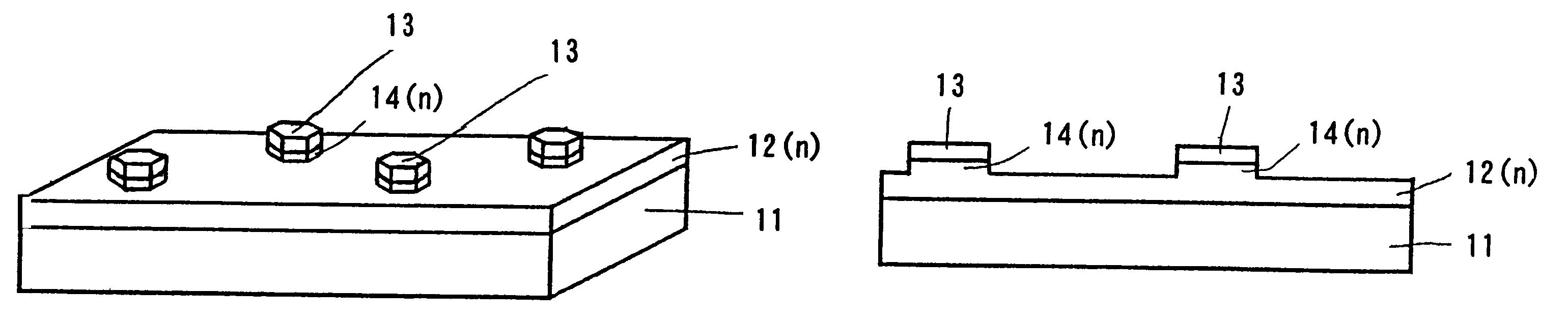
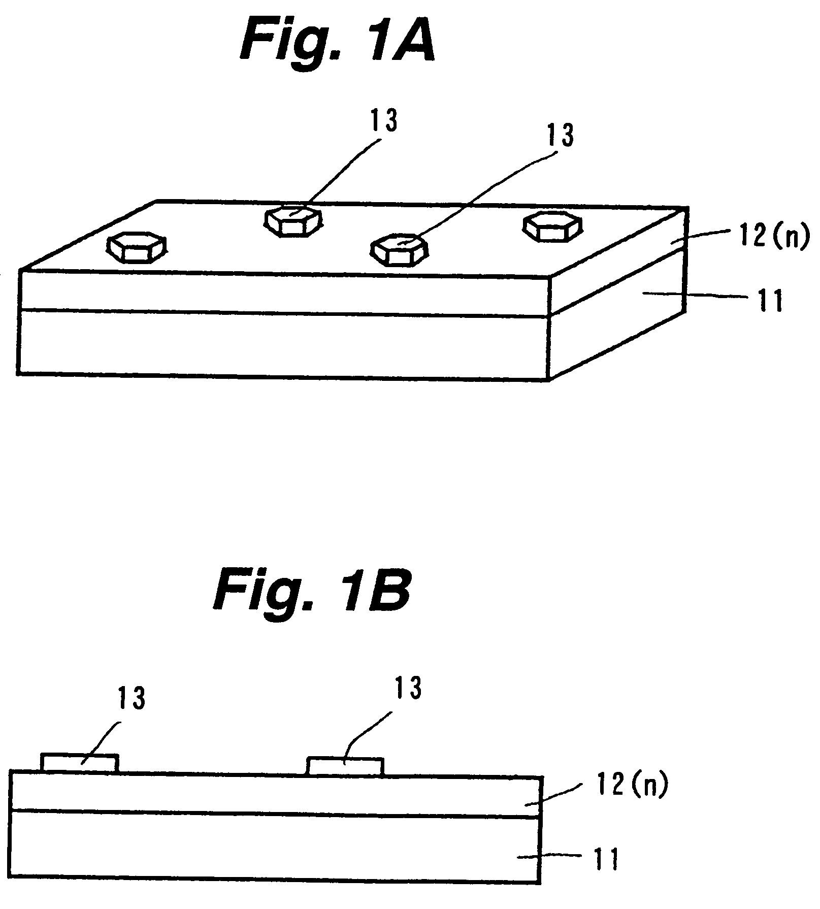
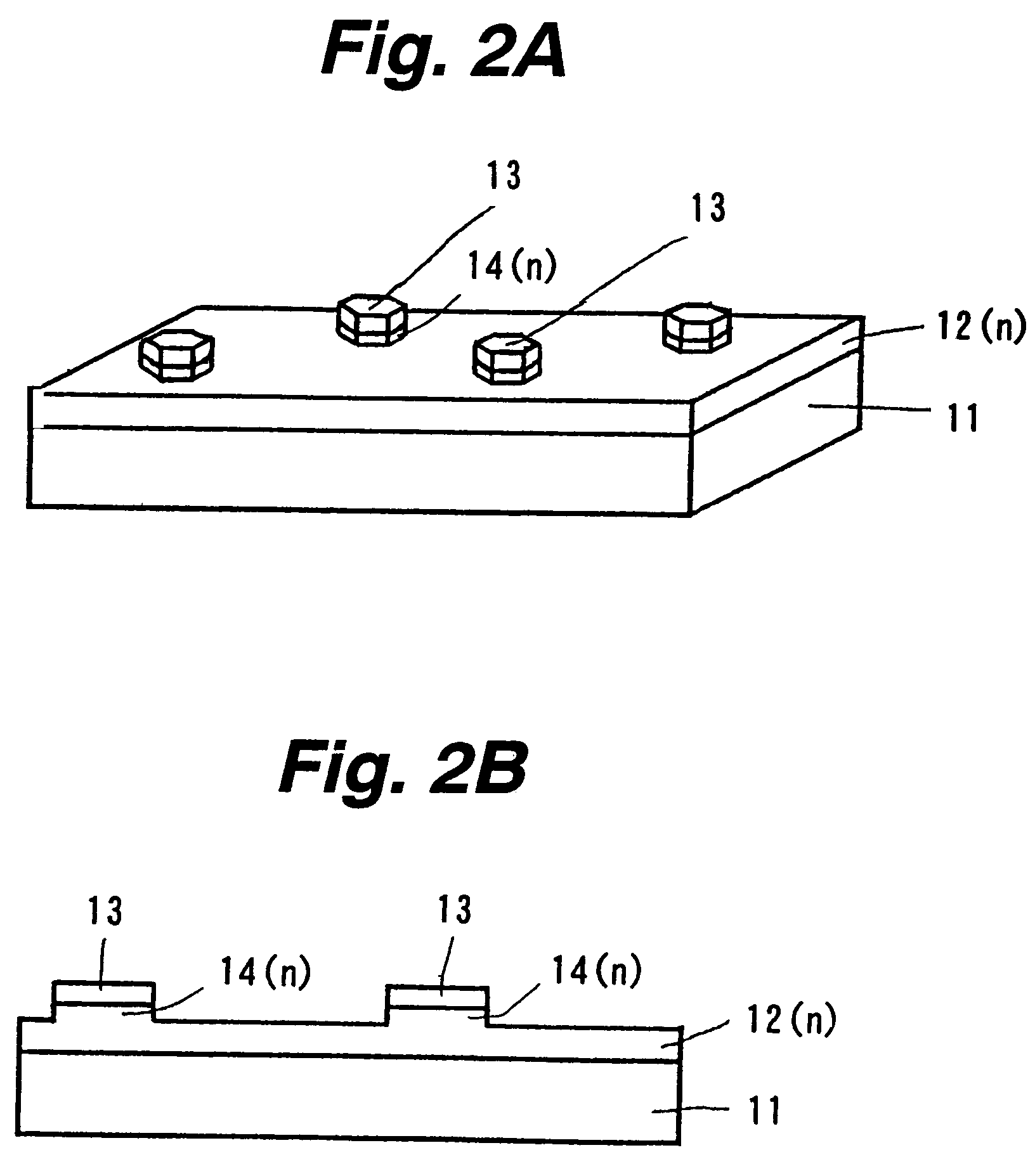
[0122]FIGS. 1A, 1B, 2A, 2B, 3A, 3B, 4A, 4B, 5A, 5B, 6A, and 6B show a manufacturing method of a GaN light emitting diode according to the invention in order of steps. FIGS. 1A, 2A, 3A, 4A, 5A, and 6A are perspective views. FIGS. 1B, 2B, 3B, 4B, 5B, and 6B are cross sectional views. FIG. 7B is a cross sectional view showing a complete state of the GaN light emitting diode.

[0123]In the first embodiment, as shown in FIGS. 1A and 1B, first, for example, a sapphire substrate 11 whose principal plane is a C+ plane is prepared and its surface is cleaned by thermal cleaning or the like. After that, an n-type GaN layer 12 in which, for example, Si has been doped as n-type impurities is grown onto the sapphire substrate 11 by, for example, an organometallic chemical vapor phase epitaxy (MOCVD) method. Although the MOCVD can be executed at any of a normal pressure, a reduced pressure, and a high pressure, it can be easily performed at the normal pressure. As an n-type GaN layer 12, it is desir...

second embodiment

[0142]A manufacturing method of a GaN light emitting diode according to the invention will now be described.

[0143]In the second embodiment, the steps are progressed and up to the process to grow the p-type GaN layer 16 is executed in a manner similar to the first embodiment and, thereafter, the p-side electrode 19 is formed onto the p-type GaN layer 16. Subsequently, by irradiating a laser beam by, for example, an excimer laser or the like from the back surface side of the sapphire substrate 11, the n-type GaN layer 12 and the portions existing on / over it are peeled off from the sapphire substrate 11. After the back surface of the n-type GaN layer 12 peeled off as mentioned above was flattened by etching or the like, the n-side electrode 18 is formed onto the back surface of the n-type GaN layer 12 as shown in FIG. 8. A transparent electrode that includes, for example, ITO or the like can be used as an n-side electrode 18. In this case, the n-side electrode 18 can be formed onto the...

third embodiment

[0146]An image display apparatus according to the present invention will now be described. The image display apparatus is shown in FIG. 10.

[0147]As shown in FIG. 10, in the image display apparatus, GaN light emitting diodes are regularly arranged in the x direction and the y direction which perpendicularly cross each other in the plane of the sapphire substrate 11, so that a 2-dimensional array of the GaN light emitting diodes is formed. A structure of each GaN light emitting diode is similar to that in, for example, the first embodiment.

[0148]The GaN light emitting diode for red (R) light emission, the GaN light emitting diode for green (G) light emission, and the GaN light emitting diode for blue (B) light emission are adjacently arranged in the y direction. One pixel is formed by those three GaN light emitting diodes. The p-side electrodes 19 of the GaN light emitting diodes for red light emission arranged in the x direction are mutually connected by a wiring 20. Similarly, the G...


PUM


Abstract

An n-type GaN layer is grown onto a sapphire substrate and a hexagonal etching mask is formed onto the n-type GaN layer as provided. The n-type GaN layer is etched to a predetermined depth by using the etching mask by the RIE method. A hexagonal prism portion whose upper surface is a C plane is formed. After the etching mask was removed, an active layer and a p-type GaN layer are sequentially grown onto the whole surface of the substrate so as to cover the hexagonal prism portion, thereby forming a light emitting device structure. After that, a p-side electrode is formed onto the p-type GaN layer of the hexagonal prism portion and an n-side electrode is formed onto the n-type GaN layer.

Description

CROSS REFERENCES TO RELATED APPLICATIONS[0001]The present application claims priority to Japanese Patent Document No. P2002-261408 filed on Sep. 6, 2002, the disclosure of which is herein incorporated by reference.BACKGROUND OF THE INVENTION[0002]The present invention relates to a semiconductor light emitting device, its manufacturing method, an integrated semiconductor light emitting apparatus, its manufacturing method, an image display apparatus, its manufacturing method, an illuminating apparatus, and its manufacturing method. More particularly, the present invention is suitable when it is applied to a light emitting diode using a compound semiconductor of a nitride III-V group.[0003]A light emitting diode in which an n-type GaN layer is grown onto a sapphire substrate, a growing mask having a predetermined opening portion is formed onto the n-type GaN layer, a hexagonal conical n-type GaN layer having an inclined crystal plane which is inclined to a principal plane of the substr...

Claims


Application Information

Patent Timeline
IPC IPC(8): H01L21/00H01L33/08H01L33/20H01L33/32H01L33/40
CPCH01L33/007H01L33/24H01L33/20
Inventor OOHATA, TOYOHARUOKUYAMA, HIROYUKIDOI, MASATOBIWA, GOSHISUZUKI, JUN
Owner SONY CORP
Why Eureka
Try Eureka