Under bump metallization pad and solder bump connections

a technology of metallization which is applied in the direction of semiconductor devices, semiconductor/solid-state device details, electrical apparatus, etc., can solve the problems of requiring a substantial requiring a large number of discrete steps, and the above-mentioned patents and prior art techniques for forming ubm pads and solder bumps are relatively complex

Inactive Publication Date: 2007-04-17
ROUND ROCK RES LLC
View PDF46 Cites 17 Cited by
  • Summary
  • Abstract
  • Description
  • Claims
  • Application Information

AI Technical Summary

Benefits of technology

[0020]In accordance with a second embodiment of the present invention, a solder bump is deposited directly on top of the flash layer on a copper bond pad on a substrate, thus eliminating the need for additional layers.

Problems solved by technology

There are problems, however, with the conventional techniques for forming UBM pads and solder bumps.
All of the above patents and prior art techniques for forming UBM pads and solder bumps are relatively complex and require a substantial number of discrete steps to form the flip chip conductive bumps.

Method used


Image

  • Under bump metallization pad and solder bump connections
  • Under bump metallization pad and solder bump connections
  • Under bump metallization pad and solder bump connections

Examples


first embodiment

[0030]FIGS. 3a–3e illustrate a preferred method of forming UBM structures and flip chip solder bump connections in accordance with the present invention. FIG. 3a shows a first metal layer 70 applied over the passivation film face surface 60 as well as the via 62 of the structure shown in FIG. 2d. Metal layer 70 is preferably formed of Titanium (Ti), and is preferably between approximately 500 to 3000 Å thick. A second metal layer 72 is applied over the first metal layer 70 as illustrated in FIG. 3b. Second metal layer 72 is preferably formed of Nickel (Ni), and is preferably between 500 and 5000 Å thick. Although FIG. 3b illustrates first layer 70 and second layer 72 preferably as being discrete layers, the invention is not so limited and only a single layer comprised of a mixture of titanium and nickel may be used. The layers 70, 72 may be applied by any method as is known in the art, such as for example by chemical vapor deposition (CVD), physical vapor deposition (PVD) sputtering...

second embodiment

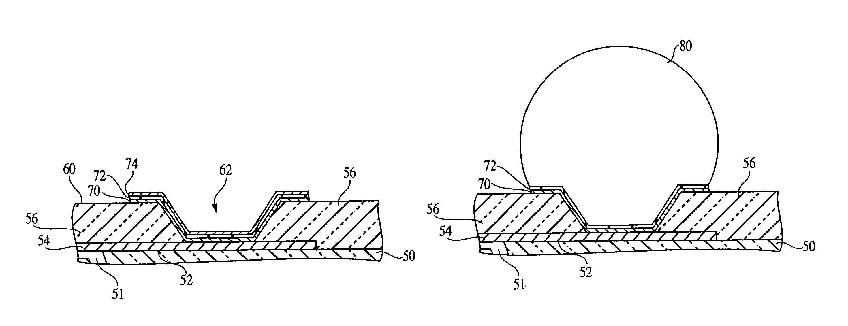
[0032]FIGS. 4a–4c illustrate a preferred method of forming a UBM pad and flip chip solder bump connections according to the present invention. In this embodiment it is preferable that the conductive traces or bond pads 54 on the semiconductor wafer face surface 52 are formed of copper. As shown in FIG. 4a, metal layer 82, preferably formed of gold (Au), silver (Ag) or palladium (Pd), is deposited or flashed over the passivation film face surface 60 as well as the via 62 of the structure shown in FIG. 2d. Metal layer 82 is preferably between 50 and 1000 Å thick.

[0033]A solder bump 80 is deposited on the layer 82 by any known industry technique, such as stenciling, screen printing, electroplating, electroless plating, evaporation, laser ball shooters, or the like as shown in FIG. 4b. Alternatively, solder bump 80 may also be formed utilizing a standard wire bonder as will be described below. When solder bump 80 is reflowed, the flash layer 82 will be consumed by solder ball 80, leavin...

third embodiment

[0034]FIGS. 5a–5c illustrate a preferred method of forming a UBM structure and flip chip solder bump connections according to the present invention. In this embodiment, a via 62 of the structure shown in FIG. 2d is plated with nickel (Ni) 84 as illustrated in 5a. It should be noted that although FIG. 5a shows the nickel plating as being at the same level as the top surface of passivation film 56, the upper surface of the nickel 84 may also be at a level which is higher or lower than the top surface of the passivation layer 56. Then, as shown in FIG. 5b, metal layer 86, preferably formed of gold (Au), is deposited or flashed over the plated nickel (Ni) 84. Although FIG. 5b shows the upper surface of metal layer 86 as being above the top surface of the passivation film 56, it could also be at the same level or below the level of the top surface of the passivation film 56.

[0035]A solder bump 80 is deposited on the layer 86 by any known industry technique, such as stenciling, screen pri...


PUM


Abstract

The present invention relates to an improved method of forming and structure for under bump metallurgy (“UBM”) pads for a flip chip which reduces the number of metal layers and requires the use of only a single passivation layer to form, thus eliminating a masking step required in typical prior art processes. The method also includes repatterning bond pad locations.

Description

[0001]This is a divisional of application Ser. No. 09 / 388,436, filed on Sep. 2, 1999 now U.S. Pat. No. 6,570,251.BACKGROUND OF THE INVENTION[0002]1. Field of the Invention[0003]The present invention relates generally to integrated circuits, and more particularly to under bump metallization pads and solder bumps on a die for flip chip type attachment to a printed circuit board or the like.[0004]2. Description of the Related Art[0005]Solder ball or bump technology is commonly used for electrical and mechanical interconnection of an integrated circuit to a substrate. High performance microelectronic devices may comprise a number of flip chips, i.e., a chip or die that has a pattern or array of terminations spaced around the active surface of the die for face-down mounting of the die to a substrate, having a Ball Grid Array (BGA) or a Slightly Larger than Integrated Circuit Carrier (SLICC). Each flip chip may be attached to a ceramic or silicon substrate or printed circuit board (PCB), ...

Claims


Application Information

Patent Timeline
Patent Type & Authority Patents(United States)
IPC IPC(8): H01L21/44H01L21/60H01L23/485
CPCH01L24/03H01L24/05H01L24/11H01L24/12H01L2224/0231H01L2224/0401H01L2224/05624H01L2224/05647H01L2224/05664H01L2224/1134H01L2224/1148H01L2224/13023H01L2224/131H01L2924/01005H01L2924/01006H01L2924/01013H01L2924/01014H01L2924/01015H01L2924/01018H01L2924/01022H01L2924/01028H01L2924/01029H01L2924/01046H01L2924/01047H01L2924/0105H01L2924/01074H01L2924/01078H01L2924/01079H01L2924/01082H01L2924/01322H01L2924/014H01L2924/05042H01L2924/10329H01L2924/14H01L2924/00014H01L2924/01024H01L2924/01033H01L2924/01087H01L2924/12042H01L2224/05559H01L2924/00
Inventor AKRAM, SALMANWOOD, ALAN G.
Owner ROUND ROCK RES LLC
Why Eureka
Try Eureka