
Electron beam apparatus and device manufacturing method using same

Inactive Publication Date: 2007-04-17
EBARA CORP
View PDF28 Cites 13 Cited by
  • Summary
  • Abstract
  • Description
  • Claims
  • Application Information

AI Technical Summary

Benefits of technology

[0015]The present invention has been proposed to solve the conventional problems mentioned above, and the present invention essentially provides an electron beam apparatus which is capable of reliably evaluating a sample such as a wafer, a mask and the like having a pattern with the minimum line width of 0.1 μm or less at a high throughput using a plurality of electron beams, i.e., multiple beams, an electron beam apparatus which comprises an electron gun for generating multiple beams using a plurality of emitter, particularly, an electron gun which is capable of accurately and readily making fine adjustments of relative positions between the plurality of emitters and a Wehnelt electrode which has holes corresponding to the plurality of emitters, and a device manufacturing method for evaluating a wafer using such an electron beam apparatus to improve the yield.
[0016]Specifically, it is a first object of the present invention to provide an electron beam apparatus which is capable of limiting aberration of a secondary optical system without the need for providing a diaphragm in the optical system.
[0017]It is a second object of the present invention to provide an electron beam apparatus for forming multiple beams using an electron gun which comprises a multi-emitter type thermal cathode with small shot noise.

Problems solved by technology

As described above, while a diaphragm is provided at a cross-over position in a primary optical system for handling a plurality of beams, problems described below arise if the diaphragm is provided in a secondary optical system.
Specifically, since the cross-over position cannot be previously predicted in the secondary optical system, a problem arises in that the diaphragm cannot be matched with the cross-over position unless an adjuster lens is provided for adjusting the cross-over position to match the position of the diaphragm.
Another problem is experienced when the diaphragm does not match the cross-over position, in which case some of a plurality of secondary electron beams closer to the optical axis are blocked by the diaphragm, so that even though the diaphragm is used to limit aberration of the optical system, the aberration cannot be reduced, resulting in a lower secondary beam detection efficiency and inability to eliminate cross-talk with adjacent beams.
However, an adjustor lens, if provided, will result in a longer optical system and require an aligner for the adjustor lens.
A further problem arises as to the need for an aligner for the diaphragm, and an astigmatism adjuster for the cross-over, resulting in a complicated configuration of the diaphragm, a larger size of the overall apparatus, a longer time needed for adjustments, and a higher cost.
However, when an array of field emission cathodes, which are inherently instable in operation, is used for an electron gun in a defect detection apparatus to generate multiple beams, even one field emission cathode in the array incapable of emission would cause the apparatus itself to fail to operate, possibly resulting in a significantly reduced operating rate.
Also, the instable operation of the field emission cathodes as mentioned above causes problems of difficulties in identifying fluctuations in emissions from the field emission cathodes and signals, and particularly, difficulties in providing an image with a large signal-to-noise ratio due to large shot noise.
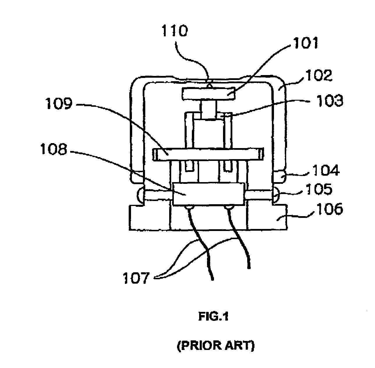
However, there are problems in applying the method of finely adjusting the relative position between the single emitter 101 and Wehnelt electrode 102 as mentioned to an electron gun which comprises a multi-emitter having a plurality of emitters.
While the inclination does not constitute a grave problem for the single emitter, the inclined multi-emitter would result in different distances between the Wehnelt electrode and all emitters, and accordingly inconsistent emissions of electrons.
A second problem, which is also true for the single emitter, is that when the entire Wehnelt electrode is moved to adjust the axial distance between the Wehnelt electrode and multi-emitter, the Wehnelt electrode can be bumped against the multi-emitter which could thereby be broken.

Method used


Image

  • Electron beam apparatus and device manufacturing method using same
  • Electron beam apparatus and device manufacturing method using same
  • Electron beam apparatus and device manufacturing method using same

Examples


first embodiment

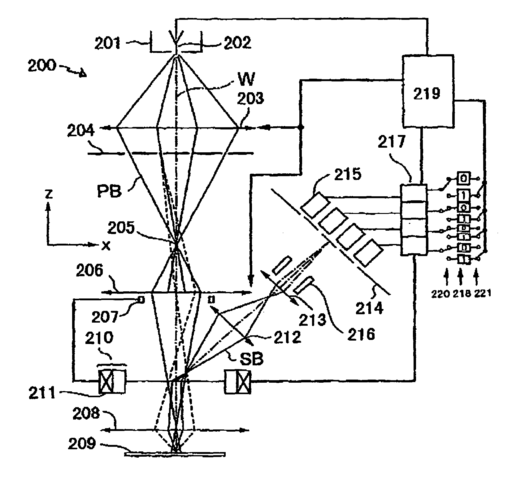
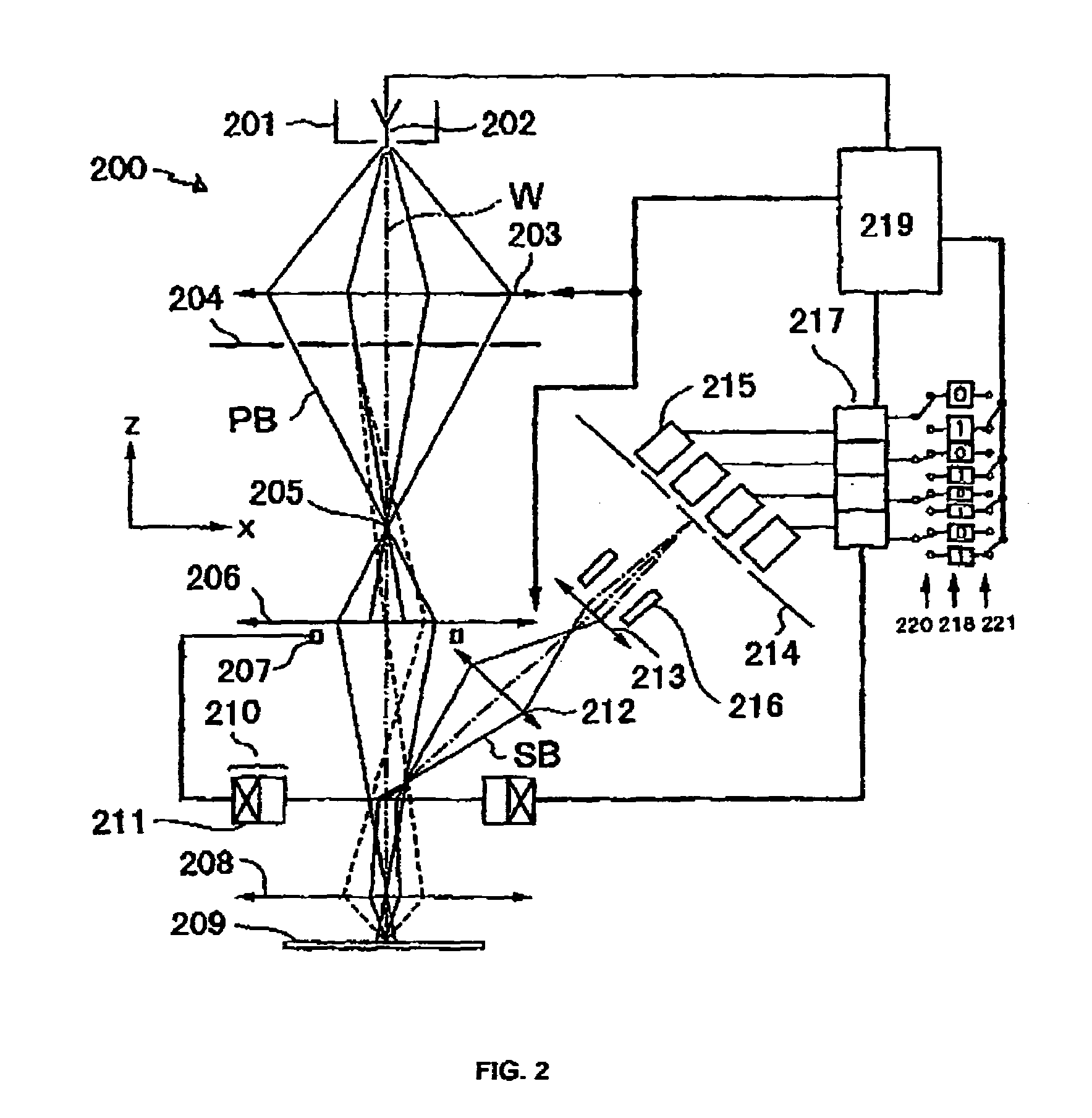
[0050]In the following, several embodiments of an electron beam apparatus according to the present invention will be described with reference to the drawings. FIG. 2 is a diagram schematically illustrating the electron beam apparatus according to the present invention. In FIG. 2, the electron beam apparatus 200 comprises an electron gun 201 as an electron beam source. An electron beam emitted from an emitter 202 of the electron gun 201 is converged by a condenser lens 203 to form a cross-over at a point 205.

[0051]A first multi-aperture plate 204 having, for example, four apertures is disposed below the condenser lens 203. The four apertures of the first multi-aperture plate 204 are formed along the circumference of the first multi-aperture plate 204. Therefore, the electron beam emitted from the electron gun 201 is irradiated to the first multi-aperture plate 204 to form four primary electron beams PB about an optical axis W.

[0052]In this way, in this embodiment, the electron gun 20...

second embodiment

[0071]FIG. 6A is a diagram schematically illustrating the electron beam apparatus according to the present invention. In FIG. 6A, electron beams emitted from an electron gun 601 of the electron beam apparatus 600 are converged by a condenser lens 602 to form a cross-over at a point 604.

[0072]Below the condenser lens 602, a first multi-aperture plate 603 having a plurality of apertures is disposed orthogonal to the optical axis W, for forming a plurality of primary electron beams. Each of the primary electron beams formed by the first multi-aperture plate 603 is reduced by a reducing lens 605, focused on and projected onto a point 606, and then focused on a sample 608 by an objective lens 607. A plurality of primary electron beams exiting from the first multi-aperture plate 603 are deflected by a deflector 609 disposed between the reducing lens 605 and objective lens 607 to simultaneously scan on the surface of the sample 608.

[0073]For eliminating the influence of field curvature abe...


PUM

PropertyMeasurementUnit
Thicknessaaaaaaaaaa
Electric fieldaaaaaaaaaa

Abstract

An electron beam apparatus including an electron gun for directing a plurality of primary electron beams onto a sample, an objective lens for forming an electric field to accelerate a plurality of secondary electron beams emitted from the sample, and a separator for separating the plurality of secondary electron beams from a primary optical system and for directing the plurality of secondary electron beams into a secondary optical system for guiding to a detector outputting a detection signal of the secondary electron beams. A deflector deflects the secondary electron beams in the secondary optical system. The deflector is controlled to deflect the plurality of secondary electron beams synchronously with scanning of the plurality of primary electron beams, thereby preventing the plurality of secondary electron beams from moving on the detector in response to the scanning of the plurality of primary electron beams.

Description

[0001]This application is a continuation of international application PCT / JP02 / 04327, filed on Apr. 30, 2002.TECHNICAL FIELD[0002]The present invention relates to a multi-beam type electron beam apparatus, and a semiconductor device manufacturing method which uses such an apparatus to evaluate wafers in the middle of processes for improving the yield. More particularly, the present invention relates to improvements on the configuration of a secondary optical system, a cathode, and an electron gun of a multi-beam type electron beam apparatus.BACKGROUND ART[0003]Generally, when aberration of an optical system must be limited to a certain value or lower, the optical system is provided with a diaphragm such that the aperture diameter of the diaphragm is adjusted to make the optical system brighter or to improve the resolution of the optical system. Also, when a plurality of beams are handled, a diaphragm is provided at a position at which a principal ray of the plurality of beams inters...

Claims


Application Information

Patent Timeline
IPC IPC(8): A61N5/00G01K1/08H01J29/70B01J35/00B01J35/04B01J35/10F01N3/28H01J37/06H01J37/28
CPCB01J35/002B01J35/04F01N3/2828H01J37/28H01J37/06F01N2330/06F01N2260/18
Inventor HAMASHIMA, MUNEKIKATO, TAKAONAKASUJI, MAMORUNOJI, NOBUHARUSATAKE, TOHRU
Owner EBARA CORP
Learn More