Semiconductor device and display comprising same

a technology of semiconductor devices and displays, applied in semiconductor devices, semiconductor/solid-state device details, electrical apparatus, etc., can solve problems such as inability to obtain performance, and achieve the effect of improving performance and versatile techniqu

Inactive Publication Date: 2007-04-17
MASASHI KAWASAKI +2
View PDF14 Cites 62 Cited by
  • Summary
  • Abstract
  • Description
  • Claims
  • Application Information

AI Technical Summary

Benefits of technology

[0024]An object of the present invention is to provide (i) a semiconductor apparatus, having a semiconductor layer that contains a group II oxide, whose performance is improved by a versatile technique; and (ii) a display apparatus including the semiconductor apparatus.
[0026]For the performance improvement of the semiconductor apparatus including the semiconductor layer containing a group II oxide such as zinc oxide or the like, the conventional techniques adopt the methods such as the crystallinity improvement, the crystallinity control of layered films, the interface control accompanied with them, and the impurity doping. On the contrary, in the arrangement according to the present invention, amorphous aluminum oxide is layered on at least one surface of the semiconductor layer. The arrangement allows the semiconductor apparatus to have performance equivalent to a semiconductor apparatus in which all the layered films are crystalline. Such performance cannot be obtained without the amorphous aluminum oxide film because the amorphous aluminum oxide layered on the semiconductor layer containing the group II oxide reduces a defect level at an interface between the semiconductor layer and the amorphous aluminum oxide. The term “defect level” indicates an electronic defect which obstructs a carrier movement in the semiconductor layer.
[0027]Therefore, it is possible to realize a semiconductor apparatus (i) in which the crystallinity improvement of the semiconductor layer made of zinc oxide or the like is less required than a conventional semiconductor apparatus; (ii) in which the film can be formed with ease; and (iii) in which a group II oxide that can be used in a large substrate with ease is used for the semiconductor layer. Further, it is possible to realize a semiconductor apparatus which has such freedom in designing that order of forming films is not fixed, and has a high versatility.
[0029]It is preferable that the semiconductor apparatus of the present invention is arranged so that the group II oxide is zinc oxide. The group II oxide for the semiconductor layer may be zinc oxide (ZnO), magnesium zinc oxide (MgxZn1−xO), cadmium zinc oxide (CdxZn1−xO), cadmium oxide (CdO), or the like. Among the group II oxides, however, zinc oxide is particularly suitable for the semiconductor layer, and is particularly expected to improve properties of the semiconductor apparatus.
[0031]According to the arrangement, the semiconductor apparatus of the present invention can have performance equivalent to a semiconductor apparatus in which all the layered films are crystalline. Further, the semiconductor apparatus ensures easy film forming. Furthermore, the semiconductor apparatus can deal with a large substrate with ease. Therefore, the semiconductor apparatus is suitably applicable to a display apparatus such as a liquid crystal display apparatus, in particular, to a large display apparatus.

Problems solved by technology

Such performance cannot be obtained without the amorphous aluminum oxide film because the amorphous aluminum oxide layered on the semiconductor layer containing the group II oxide reduces a defect level at an interface between the semiconductor layer and the amorphous aluminum oxide.

Method used


Image

  • Semiconductor device and display comprising same
  • Semiconductor device and display comprising same
  • Semiconductor device and display comprising same

Examples


first embodiment

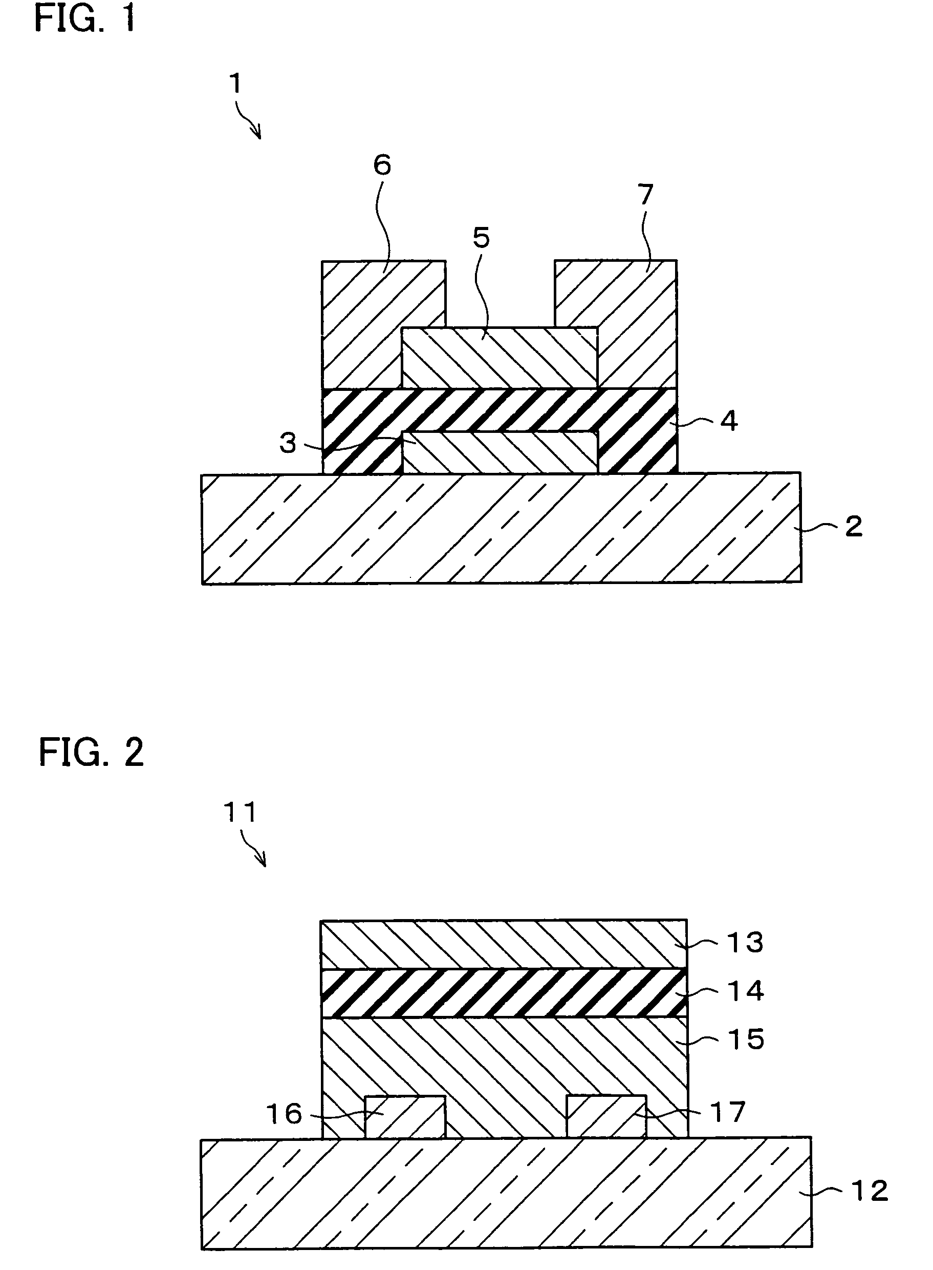
[0040][First Embodiment]

[0041]The following description discusses an embodiment of the present invention with reference to FIG. 1.

[0042]FIG. 1 is a cross sectional view illustrating a structure of a field effect transistor (FET) 1, which is a semiconductor apparatus of an embodiment of the present invention. The FET 1 is an inverse-staggered MOSFET (metal oxide semiconductor field effect transistor). Schematically, in the FET 1, a gate layer 3, a gate insulating layer 4, a channel layer 5 are layered on a substrate 2 in this order. And then, a source layer 6 and a drain layer 7 are layered thereon.

[0043]The substrate 2 serves as a base on which the layers are provided. A material of the substrate 2 may be silicon wafer, glass, plastic, or the like, and is not particularly limited in the present invention. The gate layer 3 is a gate wire for driving the FET 1, and a material of the gate layer 3 is a conductive material such as metal, semiconductor, or the like, and is not particularl...

second embodiment

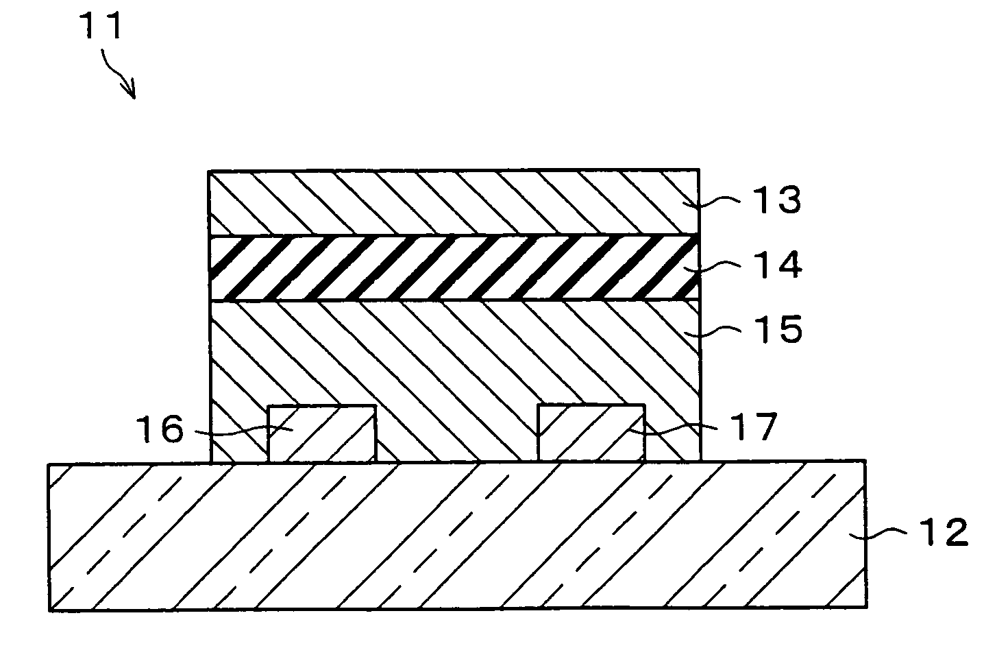
[0059][Second Embodiment]

[0060]The following description discusses another embodiment of the present invention with reference to FIG. 2.

[0061]FIG. 2 is a cross sectional view illustrating a structure of an FET 11, which is a semiconductor apparatus of the another embodiment of the present invention. The FET 11 is a staggered MOSFET. Schematically, in the FET 11, a source layer 16 and a drain layer 17 are layered on a substrate 12. Then, a channel layer 15, a gate insulating layer 14, and a gate layer 13 are layered in this order on them formed on the substrate 12. The substrate 12 and the layers 13 through 17 have equivalent functions, materials, and thickness to the substrate 2 and the layers 3 through 7 in the FET 1 (see FIG. 1), respectively. Therefore, explanations of them are omitted here.

[0062]Apparently from a comparison between the structures of FIG. 1 and FIG. 2, either the gate insulating layers 4 and 14 or the channel layers 5 and 15 can be firstly formed. This ensures mo...

third embodiment

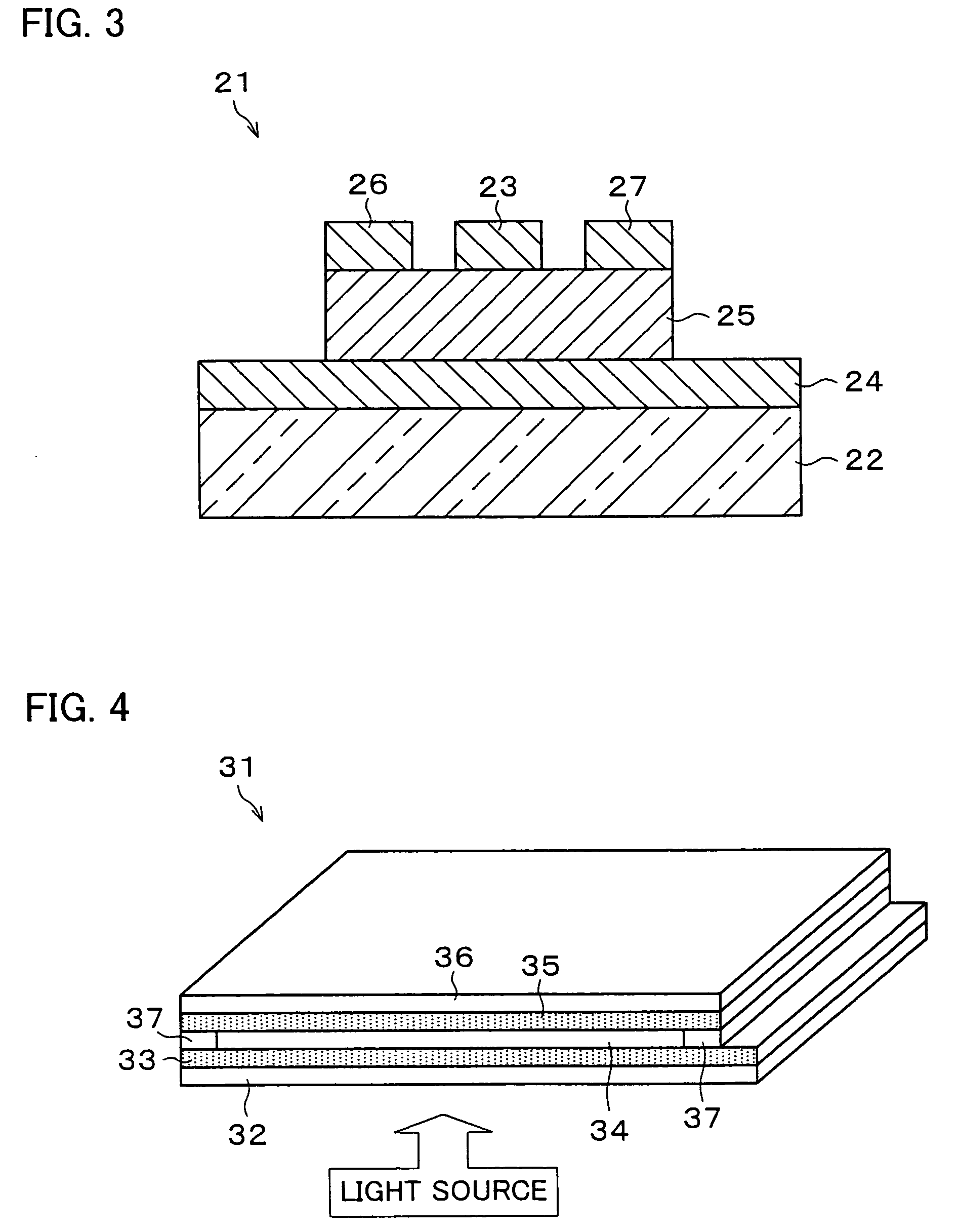
[0064][Third Embodiment]

[0065]The following description discusses still another embodiment of the present invention with reference to FIG. 3.

[0066]FIG. 3 is a cross sectional view illustrating a structure of FET 21, which is a semiconductor apparatus of the still another embodiment of the present invention. The FET 21 is a Schottky-gate FET. Schematically, in the FET 21, a priming layer 24, and a channel layer 25 are layered on a substrate 22 in this order. Further, a gate layer 23, a source layer 26 and a drain layer 27 are layered on the channel layer 25.

[0067]Like the substrates 2 and 12, the substrate 22 serves as a base for mounting the layers 23 through 27 thereon. A material of the substrate 22 is not particularly limited in the present invention, and may be silicon wafer, glass, plastic, or the like. As described above, in the case where the priming layer 24 is formed on the substrate 22, the substrate 22 normally has a film thickness not less than 0.1 mm but not more than 2...


PUM


Abstract

In an inverse-stagger MOSFET (1), a gate insulating layer (4) made of amorphous aluminum oxide is so formed as to face a channel layer (5) which serves as the semiconductor layer, and which is made of zinc oxide. With this arrangement, a defect level at an interface between the channel layer (5) and the gate insulating layer (4) is reduced, thereby obtaining performance equivalent to that of a semiconductor apparatus in which all the layered films are crystalline. This technique is applicable to a staggered MOSFET and the like, and has high versatility.

Description

[0001]This application is the U.S. national phase of international application PCT / JP03 / 03709 filed Mar. 26, 2003 which designated the U.S. and claims benefit of JP 2002-148238, dated May 22, 2002, the entire content of which is hereby incorporated by reference.TECHNICAL FIELD[0002]The present invention relates to a semiconductor apparatus in which a group II oxide is used for a semiconductor layer, and to a display apparatus including the semiconductor apparatus, and in particular to a technique for improving performance of a semiconductor apparatus in which zinc oxide is used for a semiconductor layer.BACKGROUND ART[0003]In recent years, researches have been carried out to manufacture a semiconductor apparatus in which a group II oxide such as zinc oxide is used as a semiconductor layer. These researches, in which improvement of a semiconductor apparatus is their object or means, have reported a number of high-quality and concrete techniques. Broadly speaking, the techniques show ...

Claims


Application Information

Patent Timeline
Patent Type & Authority Patents(United States)
IPC IPC(8): H01L23/58H01L29/49H01L29/786
CPCH01L29/4908H01L29/7869H01L2924/0002H01L2924/00H01L27/1225
Inventor YOSHIOKA, HIROTOFUJITA, TATSUYAOCHI, HISAOSUGIHARA, TOSHINORIHARA, TAKESHIKAWASAKI, MASASHIOHNO, HIDEO
Owner MASASHI KAWASAKI
Why Eureka
Try Eureka