High speed memory system

a memory system and high-speed technology, applied in the field of memory systems, can solve the problems of not reducing the cost of using sram cells to store memory bits, new drams are still not suitable for second-level cache operations, and drams are generally not considered to be suitable for high-speed operations, etc., to achieve the effect of increasing the width of the data input port, reducing the cost of sram cells, and increasing the storage capacity

Inactive Publication Date: 2007-04-17
INVENSAS CORP
View PDF20 Cites 2 Cited by
  • Summary
  • Abstract
  • Description
  • Claims
  • Application Information

AI Technical Summary

Benefits of technology

[0021]When accessing the DRAM array of the present invention, row access and column decoding operations are performed in a self-timed asynchronous manner. Predetermined sequences of column select operations are then performed, wherein the column select operations are synchronous with respect to a clock signal. This asynchronous-synchronous accessing scheme reduces the access latency of the DRAM array.
[0032]The DRAM array, unlike the SRAM array, also requires periodic refresh operations to restore the charge in the cell capacitors to guarantee data integrity. To manage the internal refresh operation of the DRAM array without disrupting normal CPU and system controller operations, a handshake (Krdy) signal is required to communicate between the DRAM cache memory and the system controller, so that the latter may delay its own operation and operation of the CPU while the DRAM array is being refreshed. In a preferred embodiment, one signal pin of the DRAM array is used to carry the handshake signal. The single pin maintains maximum compatibility with standard PBSRAM system controllers.

Problems solved by technology

DRAMs are generally not considered to be suitable for high speed operation because DRAM accesses inherently require a two-step process having access times ranging from 50 to 120 ns and cycle times ranging from 90 to 200 ns.
Such performance enhancement, however, does not reduce the cost of using SRAM cells to store memory bits.
These new DRAMs are still not suitable for second level cache operation, however, because their initial access time and random access cycle time remain much slower than necessary.

Method used


Image

  • High speed memory system
  • High speed memory system
  • High speed memory system

Examples


Embodiment Construction

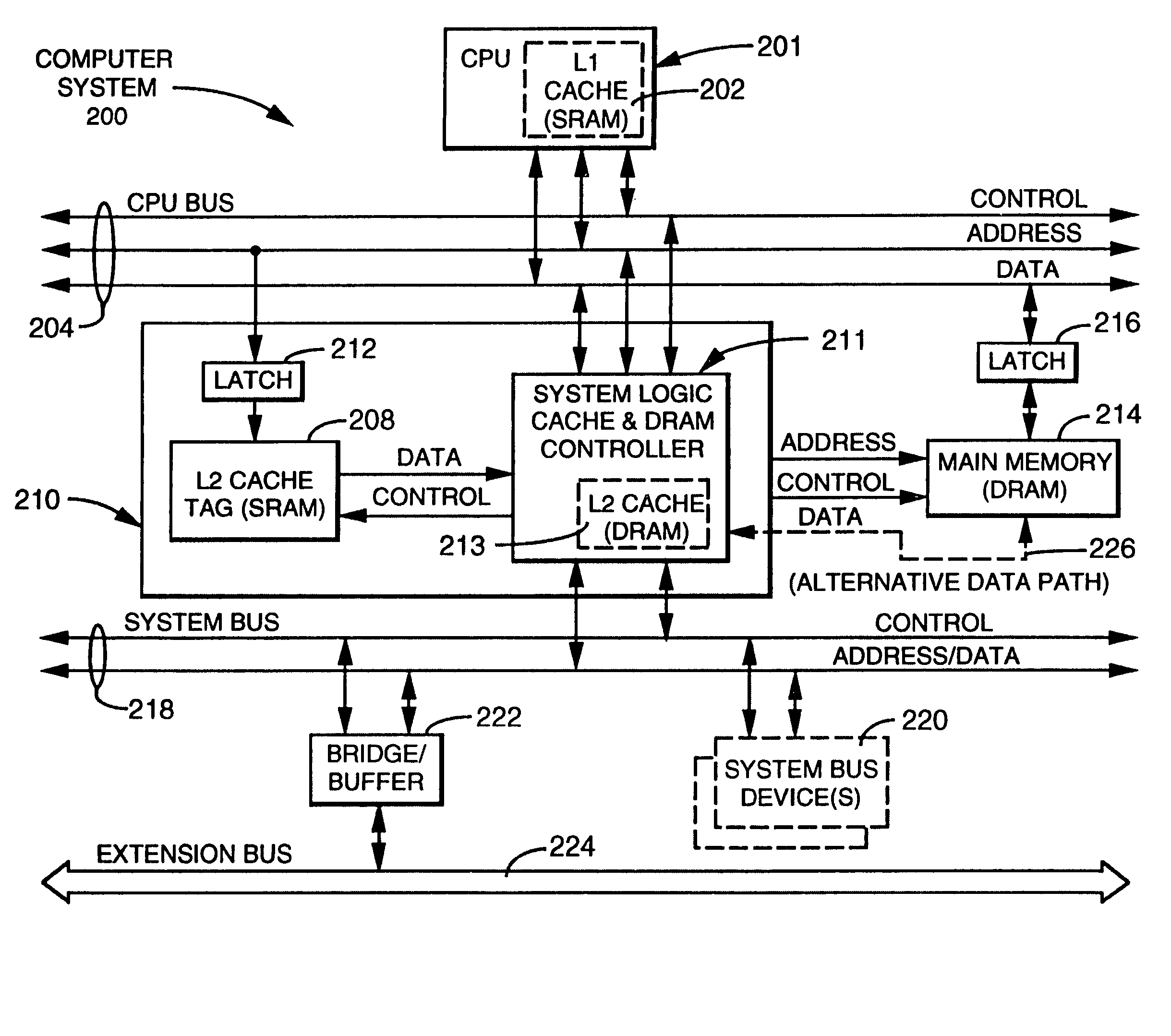
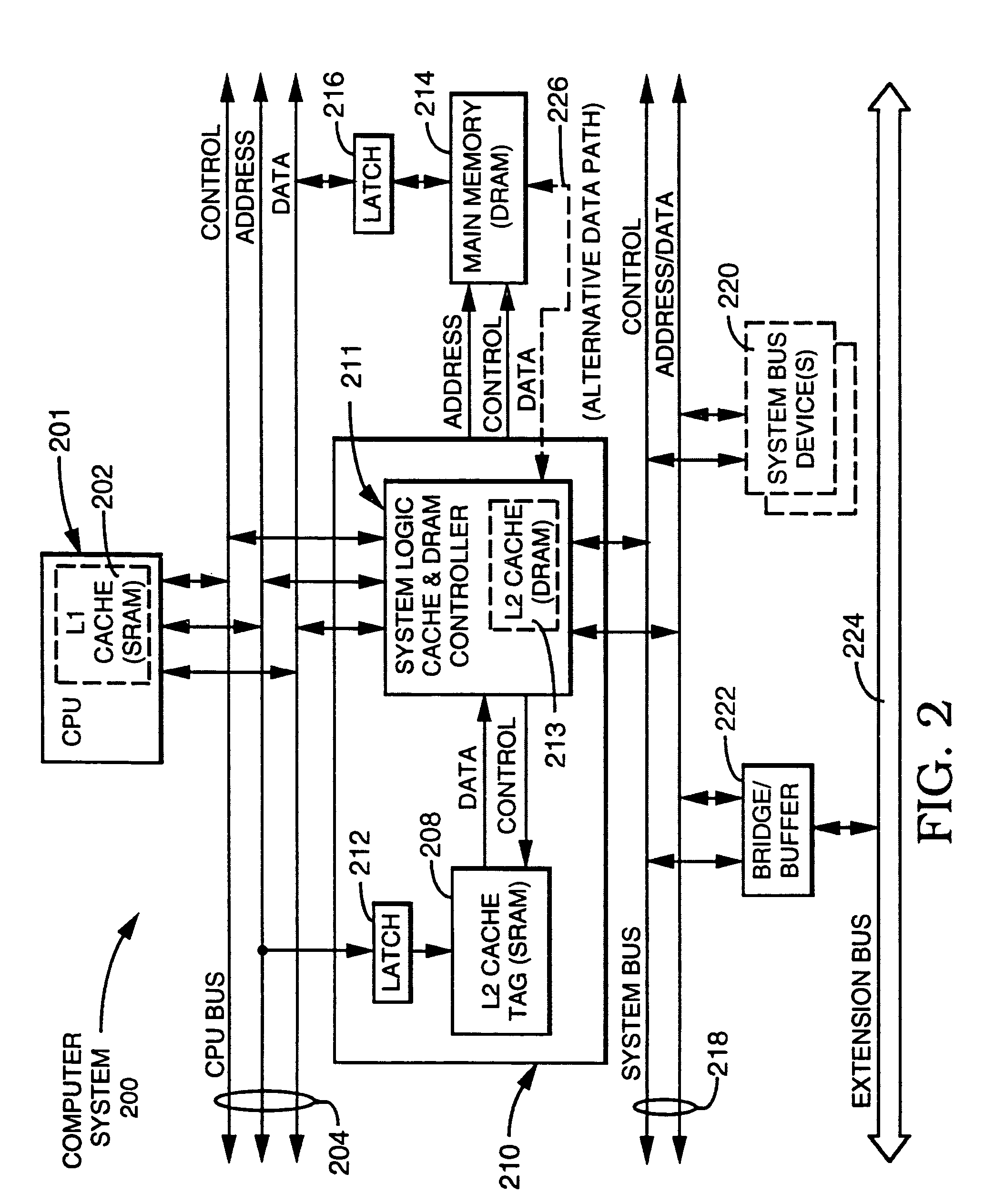
[0052]FIG. 2 is a block diagram of computer system 200 which includes second level DRAM cache memory 213 in accordance with the invention. In addition to second level DRAM cache memory 213, computer system 200 includes CPU 201, first level SRAM cache 202, CPU bus 204, latches 212 and 216, second level SRAM cache tag memory 208, system logic controller 211, main DRAM memory 214, system bus 218, bridge buffer circuit 222, system bus devices 220 and extension bus 224.

[0053]Although DRAM cache memory 213 is referred to as a “second level” cache memory, it is understood that the present invention can also be applicable to other “levels” of cache memory higher than the second level (e.g., third level or fourth level). In general, the present invention is applicable to the “next level” cache memory, where the “next level” cache memory is defined as the cache memory which is connected between the processor and a large-capacity main memory (where the main memory is typically DRAM). Using thi...


PUM


Abstract

A method and structure for implementing a DRAM memory array as a second level cache memory in a computer system. The computer system includes a central processing unit (CPU), a first level SRAM cache memory, a CPU bus coupled to the CPU, and second level cache memory which includes a DRAM array coupled to the CPU bus. When accessing the DRAM array, row access and column decoding operations are performed in a self-timed asynchronous manner. Predetermined sequences of column select operations are then performed in a synchronous manner with respect to a clock signal. A widened data path is provided to the DRAM array, effectively increasing the data rate of the DRAM array. By operating the DRAM array at a higher data rate than the CPU bus, additional time is provided for precharging the DRAM array. As a result, precharging of the DRAM array is transparent to the CPU bus.

Description

RELATED APPLICATIONS[0001]This is a divisional of U.S. patent application Ser. No. 10 / 329,015 entitled “High Speed Memory System,” filed Dec. 23, 2002 now abandoned by Fu-Chieh Hsu and Wingyu Leung, which is a continuation of application Ser. No. 09 / 851,713 filed May 8, 2001, now U.S. Pat. No. 6,510,492 entitled “Apparatus For Controlling Data Transfer Between A Bus And Memory Array And Method For Operating Same,” by Hsu, et al., which is a continuation of application Ser. No. 09 / 153,099, filed Sep. 14, 1998, now U.S. Pat. No. 6,295,593 entitled “Method Of Operating Memory Array With Write Buffers And Related Apapratus,” by Hsu, et al., which is a continuation of application Ser. No. 08 / 942,254, filed Oct. 1, 1997, now U.S. Pat. No. 6,128,700 entitled “System Utilizing A DRAM Array As A Next Level Cache Memory And Method For Operating Same,” by Hsu, et al., which is a continuation of U.S. patent application Ser. No. 08 / 443,998 filed May 17, 1995, now abandoned, entitled “Method And ...

Claims


Application Information

Patent Timeline
Patent Type & Authority Patents(United States)
IPC IPC(8): G06F12/00G06F12/06G06F12/08
CPCG06F12/0855G06F12/0879G06F12/0893G06F12/0897G06F12/10G11C7/10G11C7/1018G11C7/1051G11C7/1069G11C7/1078G11C7/1096G11C11/406G11C11/4076G11C11/4096
Inventor HSU, FU-CHIEHLEUNG, WINGYU
Owner INVENSAS CORP
Why Eureka
Try Eureka