Chip debugging using incremental recompilation and register insertion

a technology of incremental recompilation and register insertion, applied in the field of routing signals, can solve the problems of intermittent failure of the pld, simulation may not be able to provide timing characteristics that are similar, and it is almost impossible to generate a simulation that accurately exercises all of the features of the pld on the actual circuit board operating in a complex system, etc., and achieves the effect of effective solution

Inactive Publication Date: 2007-04-17
ALTERA CORP
View PDF68 Cites 150 Cited by
  • Summary
  • Abstract
  • Description
  • Claims
  • Application Information

AI Technical Summary

Benefits of technology

[0016]Where feasible, the first register is added to the I/O atom of the output pin where the signal is to be viewed. In other architectures where registers are not available in the I/O atom of an output pin, the register is placed as close possible to the I/O atom. In one particular embodiment, a single register is added for all signals of a bus to be synchronized, plus additional registers are added to those particular signals that need to be delayed further to provide synchronization. The present technique allows flexibility for the user to manage these registers while providing an effective solution to the synchronization of bus signals to be debugged. The added registers and connections can subsequently be removed to restore the original placement and routing once debugging has been successful.
[0017]The present invention provides numerous advantages in its embodiments. The user is given control over which signals should be debugged and how many registers should be inserted in a particular debugging connection path. The user also has the ability to select any of a number of clock signals to be used to clock a set of registers. Inserted registers are automatically placed and routed without disturbing the existing placement and r

Problems solved by technology

And although a simulation may be used to debug many aspects of a PLD, it is nearly impossible to generate a simulation that will accurately exercise all of the features of the PLD on an actual circuit board operating in a complex system.
For example, a simulation may not be able to provide timing characteristics that are similar to those that will actually be experienced by the PLD in a running system; e.g., simulation timing signals may be closer or farther apart than what a PLD will actually experience in a real system.
In addition to the difficulties in generating a comprehensive simulation, circuit board variables such as temperature changes, capacitance, noise, and other factors may cause intermittent failures in a PLD that are only evident when the PLD is operating within a working system.
Still further, it can be difficult to generate sufficiently varied test vectors to stress the PLD design to the point where most bugs are likely to be observed.
For example, a PLD malfunction can result when the PLD is presented with stimuli that the designer did not expect, and therefore did not take into accou

Method used


Image

  • Chip debugging using incremental recompilation and register insertion
  • Chip debugging using incremental recompilation and register insertion
  • Chip debugging using incremental recompilation and register insertion

Examples


Embodiment Construction

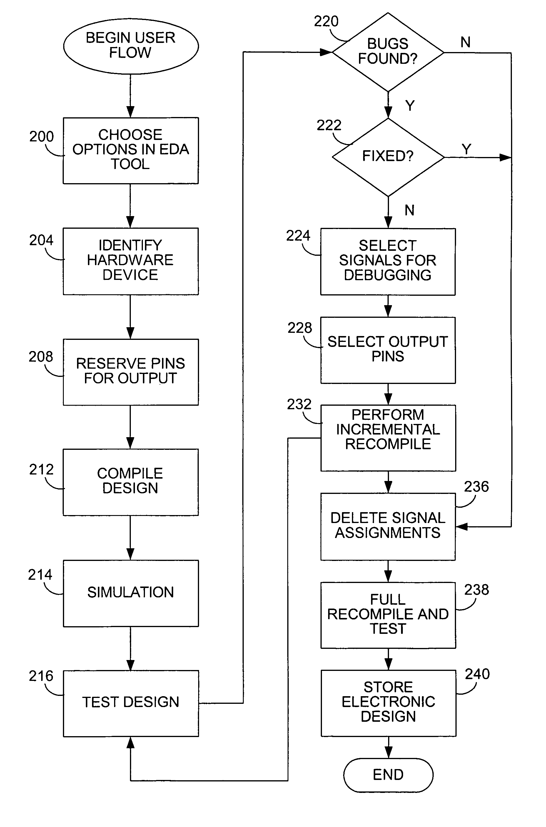
[0033]In order to develop an electronic design for programming a hardware device such as a programmable logic device (PLD), a programmable logic development system is used. As used herein, “electronic design” refers to designs for circuit boards and systems including multiple electronic devices and multi-chip modules, as well as integrated circuits. For convenience, the following discussion will generally refer to “integrated circuits,” or to “PLDs,” although the invention is not so limited.
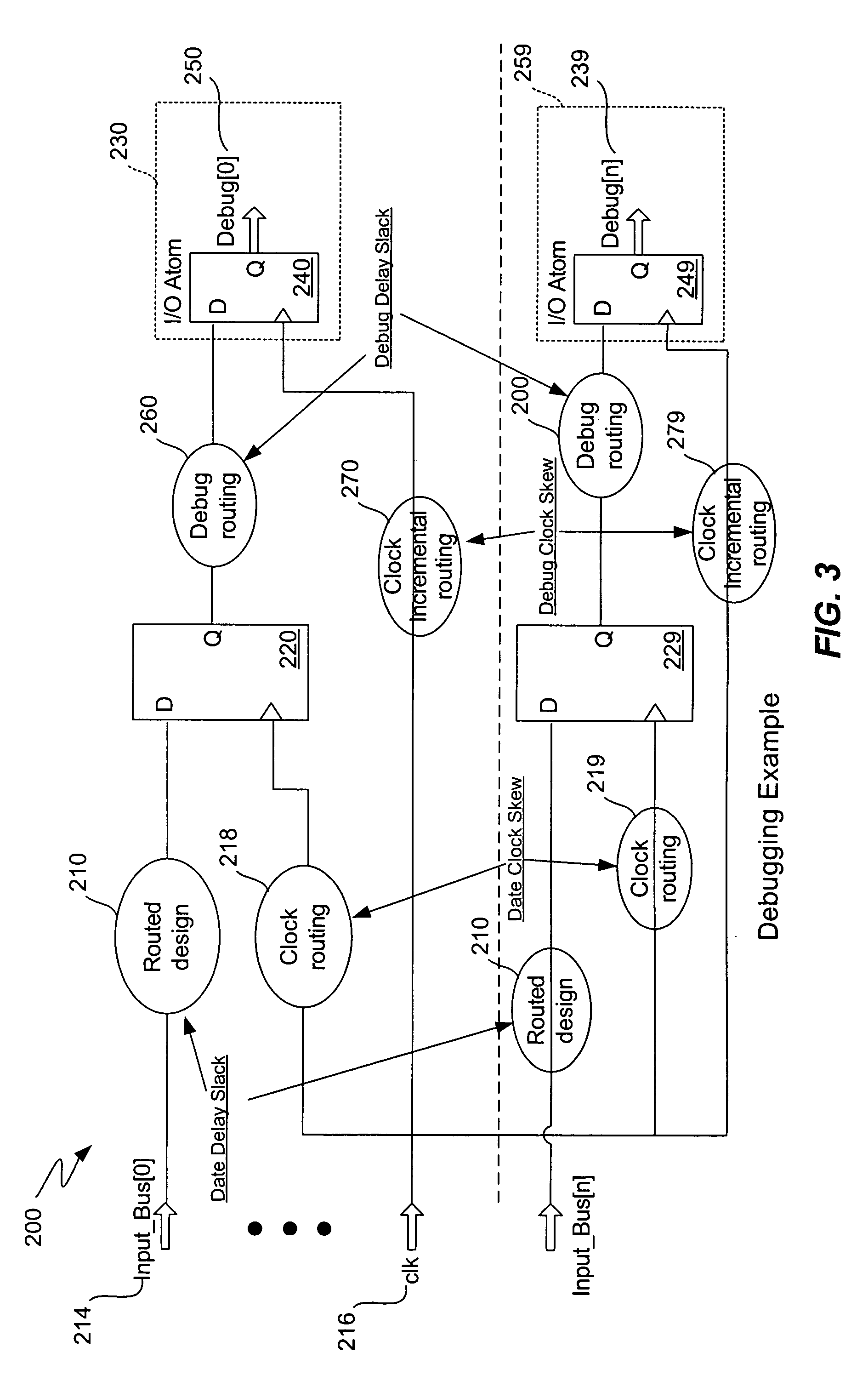
Debugging Example

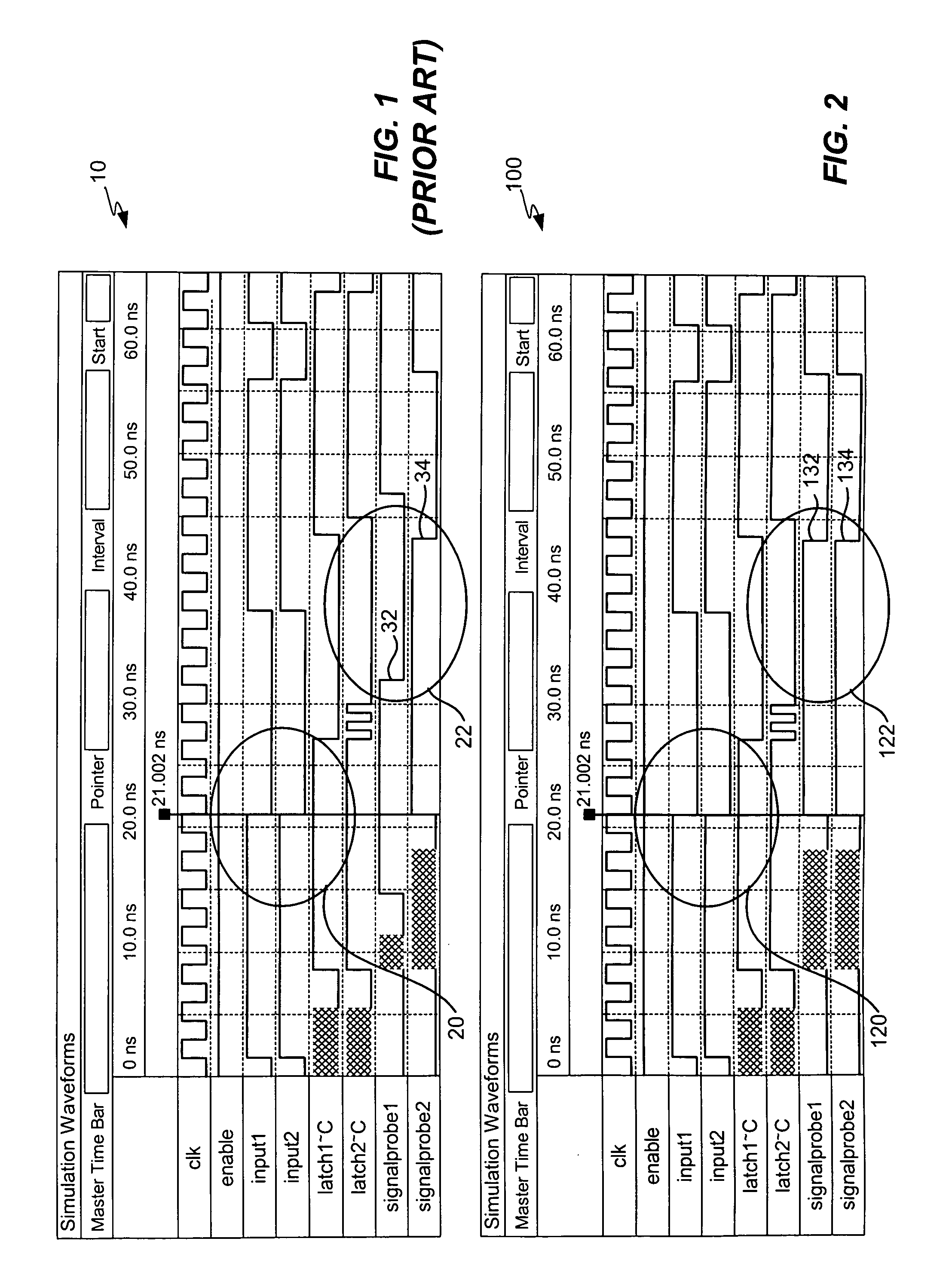
[0034]FIG. 2 illustrates timing waveforms for two signals to be debugged according to the present invention. Similar to FIG. 1, FIG. 2 shows two internal signals of a device, namely, “input1” and “input2” that are to be debugged. In this example, the present invention has been used to insert any number registers into the signal path of these signals between their source and an output pin. At the output pins, these internal signals are labeled “signalprobe1” and “signalprobe2.” In...


PUM


Abstract

While debugging, a user chooses an incremental recompile. Internal signals of interest and output pins are selected, and a number of additional registers are chosen to insert in the path of each internal signal. A clock is selected for the registers. An incremental recompile of the compiled design compiles a routing from each internal signal to an output pin via the added registers. The database building and logic synthesis stages are skipped. The post-fitting logical netlist and routing netlist are retrieved. The new registers are created and the internal signal is connected to the output pin atom in the logical netlist. The fitter places and routes the connections to create a new routing netlist and then the new routing netlist is output into a programming output file (POF) in a form suitable for programming the PLD. The original routing netlist is undisturbed. The user views the internal signals at the output pins chosen. The user may iterate through this process many times in order to debug the PLD. The debugging assignments may be deleted.

Description

FIELD OF THE INVENTION[0001]The present invention relates generally to analysis of a hardware device in connection with a computer system. More specifically, the present invention relates to routing signals within a programmable logic device for purposes of debugging.BACKGROUND OF THE INVENTION[0002]In the field of electronics various electronic design automation (EDA) tools are useful for automating the process by which integrated circuits, multi-chip modules, boards, etc., are designed and manufactured. In particular, electronic design automation tools are useful in the design of standard integrated circuits, custom integrated circuits (e.g., ASICs), and in the design of custom configurations for programmable integrated circuits. Integrated circuits that may be programmable by a customer to produce a custom design for that customer include programmable logic devices (PLDs). Programmable logic devices refer to any integrated circuit that may be programmed to perform a desired funct...

Claims


Application Information

Patent Timeline
IPC IPC(8): G06F11/00
CPCG01R31/318364
Inventor MARTI, PHILIPPEJERVIS, MARKNIXON, GREGOR
Owner ALTERA CORP
Why Eureka
Try Eureka