Semiconductor device with an enhancement type field effect transistor in which threshold voltage is dependent upon substrate bias voltage

a semiconductor device and enhancement technology, applied in transistors, solid-state devices, pulse techniques, etc., can solve the problems of increasing the surface area of the wiring layer, increasing the power consumption of the semiconductor integrated circuit when the integrated circuit is not operating, and increasing the leak current. , to achieve the effect of simple process

Inactive Publication Date: 2007-04-24
LAPIS SEMICON CO LTD
View PDF7 Cites 11 Cited by
  • Summary
  • Abstract
  • Description
  • Claims
  • Application Information

AI Technical Summary

Benefits of technology

[0013]According to the semiconductor integrated circuit relating to the first invention, the threshold value voltage of the third field effect transistor can be controlled by controlling the substrate voltage, and hence the leak current when this circuit is not operating can be reduced.
[0021]According to the fifth invention, the semiconductor device relating to the fourth invention can be fabricated by means of a simple process.

Problems solved by technology

However, the lower the threshold value voltage, the greater the leak current when the field effect transistor is turned OFF.
For this reason, when the threshold value voltage is lowered, the power consumption when the semiconductor integrated circuit is not operating increases.
Consequently, there is the drawback that the surface area of the wiring layer increases.
Hence, there is the drawback that the withstand voltage of the nMOS transistor 630 then drops due to the parasitic bipolar effect.
On the other hand, the semiconductor integrated circuit disclosed in Japanese Patent Application Laid Open No. 05-268027 must be a circuit for controlling the back gate bias by detecting an increase in the penetration current, and there is therefore the drawback that the circuit scale is then extremely large.

Method used


Image

  • Semiconductor device with an enhancement type field effect transistor in which threshold voltage is dependent upon substrate bias voltage
  • Semiconductor device with an enhancement type field effect transistor in which threshold voltage is dependent upon substrate bias voltage
  • Semiconductor device with an enhancement type field effect transistor in which threshold voltage is dependent upon substrate bias voltage

Examples


first embodiment

[0030

[0031]First of all, the first embodiment of the present invention will be described by using FIGS. 1 to 3.

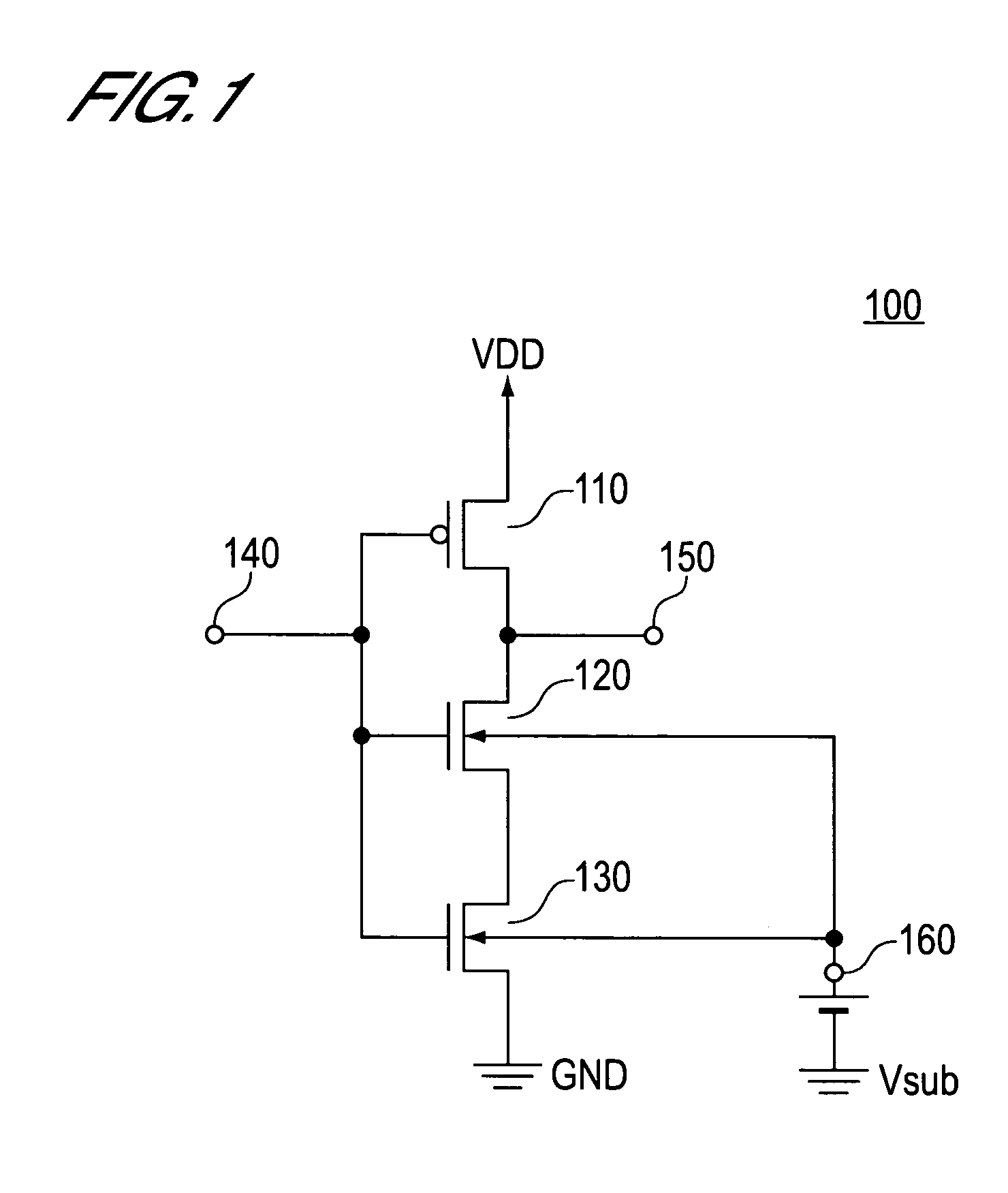
[0032]FIG. 1 is a circuit diagram that shows an example in which the present embodiment is applied to an inverter with a CMOS (Complementary Metal Oxide Semiconductor) structure.

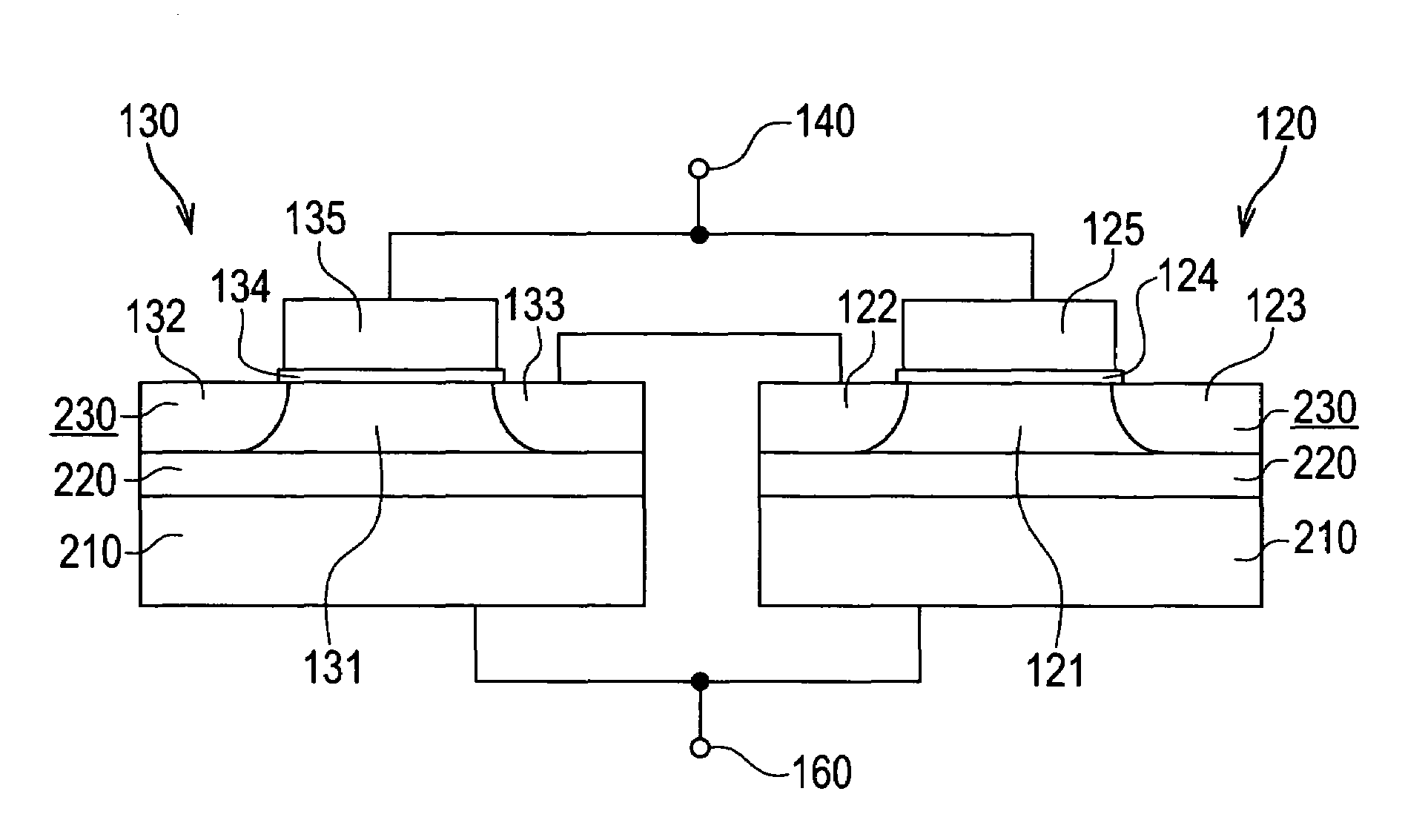
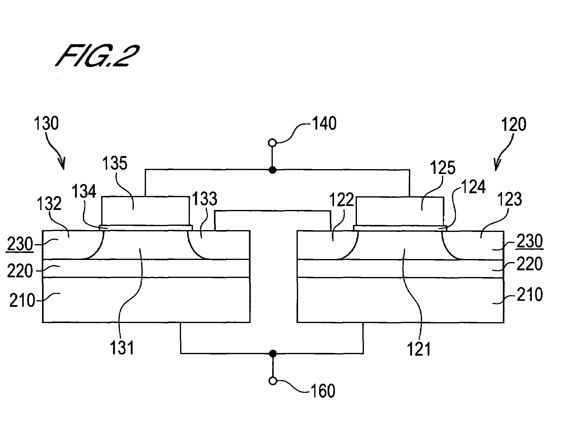
[0033]As shown in FIG. 1, this inverter 100 comprises a pMOS transistor 110, an nMOS transistor 120, and a leak-current prevention nMOS transistor 130.

[0034]The pMOS transistor 110 is connected such that the source thereof is connected to a power supply line VDD, the drain is connected to a signal output terminal 150, and the gate is connected to a signal input terminal 140. In this embodiment, an enhancement mode pMOS transistor having a p+ polysilicon gate is used as the pMOS transistor 110.

[0035]The nMOS transistor 120 is connected such that the drain thereof is connected to the signal output terminal 150, and the gate is connected to the signal input terminal 140. Further, a substrate voltage Vs...

second embodiment

[0058

[0059]Next, the second embodiment of the present invention will be described by using FIGS. 4 and 5.

[0060]This embodiment is an example in which an enhancement mode nMOS transistor employing an n+ polysilicon gate (equivalent to the nMOS transistor 120 of FIGS. 1 and 2) and a depression mode nMOS transistor (equivalent to the nMOS transistor 130 in FIGS. 1 and 2) employing a midgap gate are integrally formed.

[0061]FIG. 4 is a cross-sectional view that schematically shows the constitution of a composite element 400 relating to this embodiment.

[0062]As shown in FIG. 4, a p-type semiconductor layer 430 is provided on a substrate 410 via an insulation film 420. An SOI substrate is therefore used in this embodiment.

[0063]The element formation region of the p-type semiconductor layer 430 is separated from the element by a field oxide film 440. Further, an intrinsic p-type impurity region 431 (1×1015 cm−3, for example) and a p-type impurity region 432 (5×1017 cm−3, for example), which...


PUM


Abstract

An enhancement mode field effect transistor whose operation threshold value varies greatly according to the substrate voltage. This field effect transistor is implemented by substituting the gate electrode of a depression mode field effect transistor for a gate electrode of the conductivity type opposite to that of a channel formation region, or a midgap gate electrode. In a preferred embodiment of the present invention, this field effect transistor is provided between a CMOS structure logic gate and a ground line. As a result, the leak current when the field effect transistor is not operating can be diminished without reducing the operational speed of the logic gate.

Description

BACKGROUND OF THE INVENTION[0001]1. Field of the Invention[0002]The present invention relates to a semiconductor integrated circuit, a semiconductor device, and a semiconductor device fabrication method and, more particularly, to technology for reducing the leak current of the semiconductor integrated circuit.[0003]2. Description of Related Art[0004]In recent years, the demand for increased intricacy in semiconductor integrated circuits has grown steadily. A reduction in the voltages of power sources has accompanied this increase in the intricacy of semiconductor integrated circuits. In order to lower the supply voltage, the threshold value voltage of the transistor constituting the semiconductor integrated circuit must be set low. For example, when the supply voltage is 1 volt, the threshold value voltage of a field effect transistor is desirably on the order of 0.2 to 0.3 volt. However, the lower the threshold value voltage, the greater the leak current when the field effect trans...

Claims


Application Information

Patent Timeline
Patent Type & Authority Patents(United States)
IPC IPC(8): H01L21/331H01L21/336H01L21/8236H01L27/08H01L21/8238H01L27/01H01L27/088H01L27/092H01L27/12H01L29/786H03K19/00
CPCH01L27/1203H01L29/66772H01L29/78609H01L29/78624H01L29/78648H03K19/0027H03K2217/0018
Inventor BABA, SHUNSUKE
Owner LAPIS SEMICON CO LTD
Why Eureka
Try Eureka