
Substrate supporting plate and stripping method for supporting plate

a technology of supporting plate and supporting plate, which is applied in the direction of solid-state devices, layered products, chemistry apparatus and processes, etc., can solve the problems of insufficient protection tape to support thinned semiconductor wafers, easy cracking or chipping of semiconductor wafers when the tape is applied, and the transfer needs to be carried out by manpower. , to achieve the effect of short period of tim

Inactive Publication Date: 2007-05-01
TOKYO OHKA KOGYO CO LTD
View PDF19 Cites 56 Cited by
  • Summary
  • Abstract
  • Description
  • Claims
  • Application Information

AI Technical Summary

Benefits of technology

The solution enables fast, crack-free stripping of semiconductor wafers with reduced warpage and allows for automated handling by using a solvent to dissolve the adhesive through the supporting plate's holes, facilitating efficient processing.

Problems solved by technology

In the case of using the protecting tape as disclosed in Document 1, cracking or chipping of the semiconductor wafer easily occurs when the tape is stripped.
Also, the protecting tape is not sufficient to support the thinned semiconductor wafer.
Consequently, transfer needs to be conducted by manpower, and automation is impossible.
However, since it is difficult for a solvent to enter between the supporting plate and the semiconductor wafer at the time of stripping, it takes too much time to strip the supporting plate from the semiconductor wafer.
Also, the thermoplastic film bonding the support plate and the semiconductor wafer often fails to completely dissolve, and tends to be left in a state of sticking to either one of the support plate and the semiconductor wafer.
However, if the circuit-formed surface of the semiconductor wafer is irradiated with the ultraviolet rays, the element (CCD or CMOS) might be damaged.
In the case of using alumina, aluminum nitride, boron nitride, or silicon carbide as the protecting base, since a magnet cannot be employed at the time of stripping, the apparatus must be complicated.

Method used


Image

  • Substrate supporting plate and stripping method for supporting plate
  • Substrate supporting plate and stripping method for supporting plate
  • Substrate supporting plate and stripping method for supporting plate

Examples


Embodiment Construction

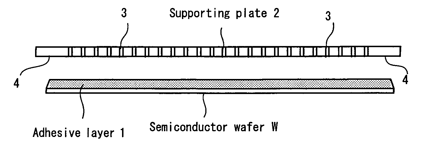
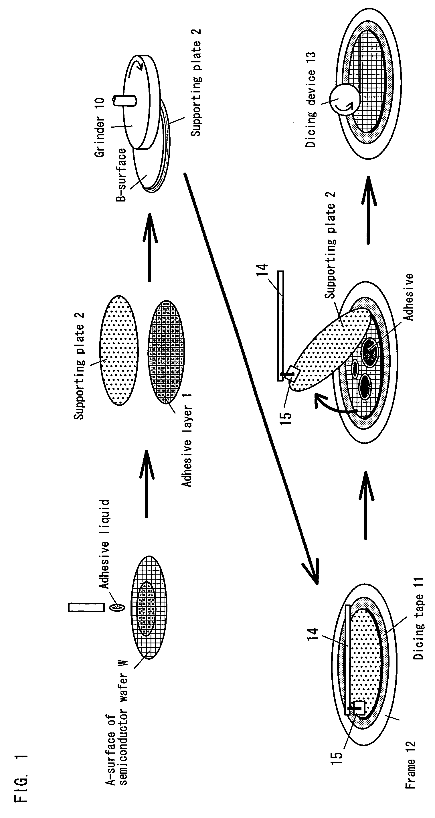
[0033]Embodiments of the present invention will be described below with reference to the attached drawings. FIG. 1 is a view showing a supporting plate according to the present invention and processes for thinning a semiconductor wafer in which a stripping method for the supporting plate is incorporated. First, an adhesive liquid is applied onto a circuit(element)-formed surface of a semiconductor wafer W. The application is conducted by using a spinner or the like. The material for the adhesive liquid is a novolac-type phenol resin.

[0034]Next, the adhesive liquid undergoes preliminary drying, so that its flowability is reduced and it can keep its shape as an adhesive layer 1. For the preliminary drying, heating is conducted for 5 minutes at a temperature of 80° C. by using an oven. The thickness of the adhesive layer 1 is determined based on the irregularities of the circuit which has been formed on the surface of the semiconductor wafer W. If a sufficient thickness is not obtained...


PUM

PropertyMeasurementUnit
temperatureaaaaaaaaaa
thicknessaaaaaaaaaa
thicknessaaaaaaaaaa

Abstract

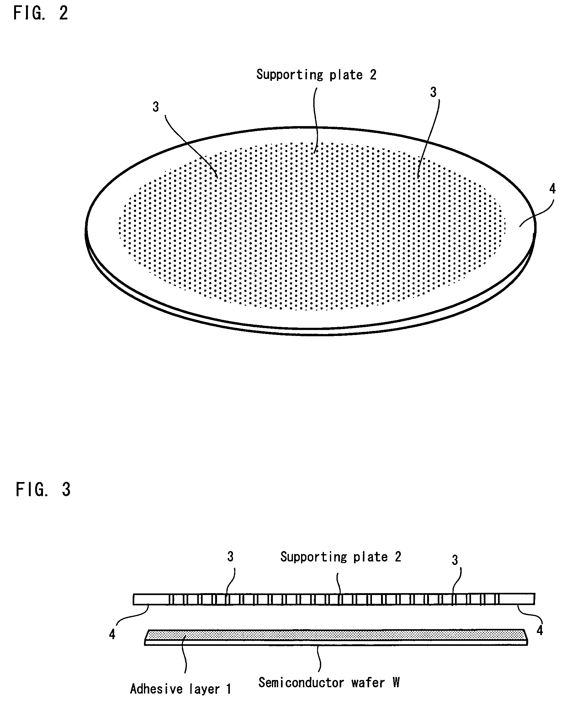
There is provided a supporting plate having a structure in which a solvent can be supplied to an adhesive layer between the supporting plate and a substrate such as a semiconductor wafer in a short period of time after the substrate is thinned, and also a method for stripping the supporting plate.The supporting plate may have a larger diameter than the semiconductor wafer, and penetrating holes are formed in the supporting plate. The outer peripheral portion of the supporting plate is a flat portion in which no penetrating hole is formed. When alcohol is poured from above the supporting plate, the alcohol reaches the adhesive layer through the penetrating holes, dissolves and removes the adhesive layer.

Description

BACKGROUND OF THE INVENTION[0001]1. Field of the Invention[0002]The present invention relates to a supporting plate which is attached to a substrate such as a semiconductor wafer to support the substrate when the substrate is thinned, and also relates to a method for stripping the supporting plate.[0003]2. Description of the Prior Art[0004]There has been a need of making IC cards for cell phones thinner, smaller, and lighter. In order to satisfy this need, a semiconductor chip to be incorporated therein must be thin. Although the thickness of a wafer which forms a semiconductor chip is 125–150 μm at present, it is expected that the thickness of a semiconductor wafer must be 25–50 μm for a next generation chip.[0005]A conventional method for thinning a semiconductor wafer is shown in FIG. 7. Specifically, a protecting tape is attached to a surface (A-surface) of a semiconductor wafer on which a circuit (element) has been formed. The wafer is turned over, and the rear surface (B-surfa...

Claims


Application Information

Patent Timeline
Patent Type & Authority Patents(United States)
IPC IPC(8): B32B38/10H01L21/304H01L21/00H01L21/02
CPCH01L21/6708H01L21/6835H01L21/6836H01L2221/68318H01L2221/68327H01L2221/68381Y10T156/1116Y10T156/11Y10T156/1147Y10T156/1911Y10T156/1928Y10T156/1111Y10S156/93H01L21/02H01L21/304
Inventor MIYANARI, ATSUSHI
Owner TOKYO OHKA KOGYO CO LTD
Learn More