Modeling interconnected propagation delay for an integrated circuit design

a propagation delay and integrated circuit technology, applied in the field of circuit modeling, can solve the problems of increasing the complexity of delay calculation, calculating a single linear resistor, and unable to model gate loads by purely capacitive loads for high-performance digital circuits

Active Publication Date: 2007-05-01
SYNOPSYS INC
View PDF7 Cites 20 Cited by
  • Summary
  • Abstract
  • Description
  • Claims
  • Application Information

AI Technical Summary

Benefits of technology

[0023]Once these parameters are identified, the process replaces the drive logic element in a linear circuit representation of the first logic stage with a current source characterized as a function of the current at the con...

Problems solved by technology

However, with the emerging interconnect dominance, gate loads can no longer be modeled by purely capacitive loads for high performance digital circuits.
The main difficulty with these approaches is calculating a single linear resistor, which captures the switching behavior of a CMOS gate.
Some methodologies use more than two points to characterize the waveshape, while others employ more complex load models—both of which increase the complexity of delay calculation significantly.
However, if one considers the same gate resistance and total load capacitance, but increases the metal resistance so that RdM, the gate delay at node vout will d...

Method used


Image

  • Modeling interconnected propagation delay for an integrated circuit design
  • Modeling interconnected propagation delay for an integrated circuit design
  • Modeling interconnected propagation delay for an integrated circuit design

Examples


Embodiment Construction

[0037]The Figures (“FIG.”) and the following description relate to preferred embodiments of the present invention by way of illustration only. It should be noted that from the following discussion, alternative embodiments of the structures and methods disclosed herein will be readily recognized as viable alternatives that may be employed without departing from the principles of the claimed invention.

Current Source for Pure Capacitance Load

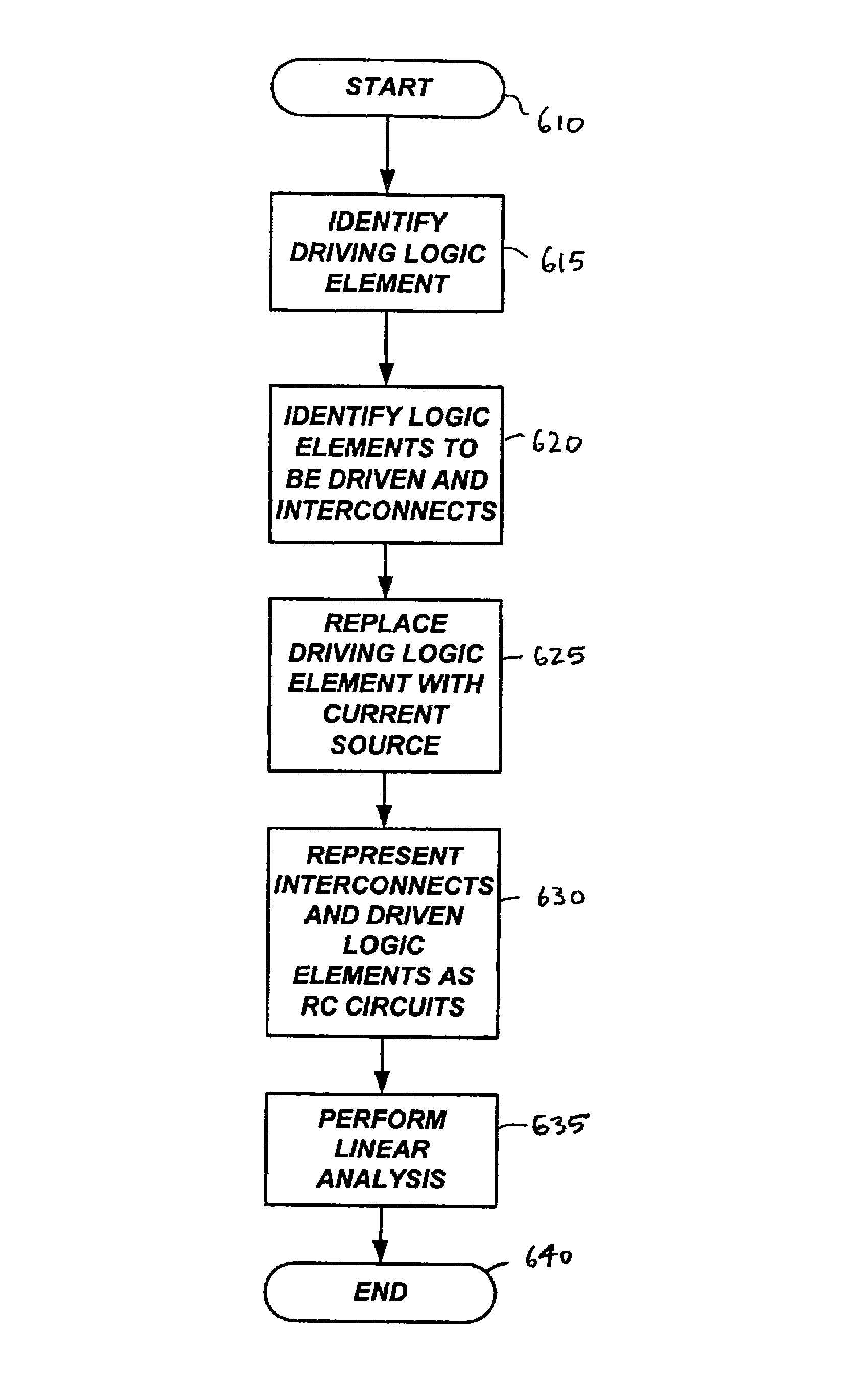
[0038]Referring now to FIG. 5, a logic stage 505 includes a driver gate 520 and driven logic inputs C 532 and D 562 and interconnects 540, 545 (note that interconnects may comprise one wire or multiple wires) between them in accordance with the present invention. The drive logic stage 505 drives subsequent logic elements in subsequent logic stages. The present invention includes a system and method for determining timing (or signal propagation delay) between an input of the drive logic stage 505 and an input of each logic element in subsequent logi...


PUM


Abstract

A system and a method are disclosed for performing a timing or signal propagation delay analysis on a circuit. The disclosure includes representing a drive logic stage as a representative linear circuit driven by a current source. The current source is represented as a function of a current at a constant value, a start time, a tail-start time, and a time constant of an equivalent capacitive circuit. Once the current source model is constructed, a logic stage can be analyzed for timing or signal propagation delay using conventional linear circuit analysis techniques. The disclosure also is applicable to resistance capacitance (“RC”) interconnect circuits using a current source model in which an RC load is represented as an effective capacitance and the current source for use in a linear analysis is constructed using an iterative approach.

Description

BACKGROUND OF THE INVENTION[0001]1. Field of the Invention[0002]The present invention generally relates to the field of circuit modeling, and more specifically, to gate delay models.[0003]2. Description of the Relevant Art[0004]To shorten design cycles, digital systems are often designed at a gate and / or cell level. In contrast to designing at a transistor level, gate or cell level design can significantly reduce costly design verification by precharacterizing gate and cell delays for static timing analysis. The cell delays and transitions are generally expressed empirically as a function of load capacitance and input signal transition time. However, with the emerging interconnect dominance, gate loads can no longer be modeled by purely capacitive loads for high performance digital circuits.[0005]For digital IC technologies in general, and CMOS in particular, it is assumed that a load at an output of the gate has a negligible impact on the waveform behavior at a gate input. Therefor...

Claims


Application Information

Patent Timeline
IPC IPC(8): G06F9/45G06F17/50
CPCG06F17/5022G06F30/33
Inventor CELIK, MUSTAFAROHRER, RONALD A.
Owner SYNOPSYS INC
Why Eureka
Try Eureka