Plasma gate oxidation process using pulsed RF source power

a technology of pulsed rf source power and oxidation process, which is applied in the direction of electrical equipment, basic electric elements, electric discharge tubes, etc., can solve the problem that the plasma itself is never fully extinguished, and achieve the effect of low defect density

Active Publication Date: 2007-05-08
APPLIED MATERIALS INC
View PDF16 Cites 35 Cited by
  • Summary
  • Abstract
  • Description
  • Claims
  • Application Information

AI Technical Summary

Problems solved by technology

The frequency of the “on” and “off” intervals is such that the plasma itself is never fully extinguished.

Method used


Image

  • Plasma gate oxidation process using pulsed RF source power
  • Plasma gate oxidation process using pulsed RF source power
  • Plasma gate oxidation process using pulsed RF source power

Examples


Embodiment Construction

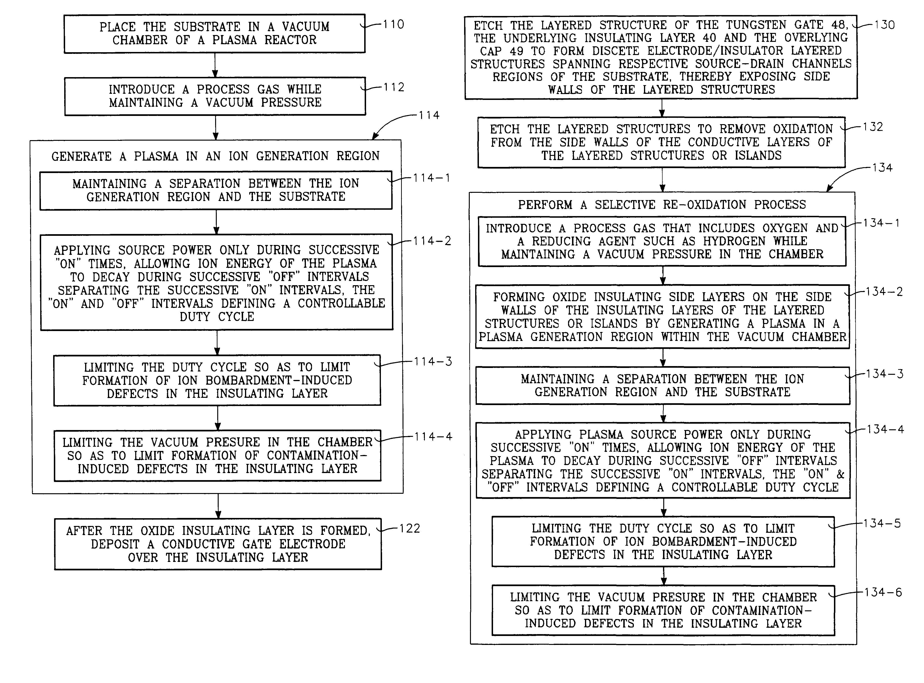
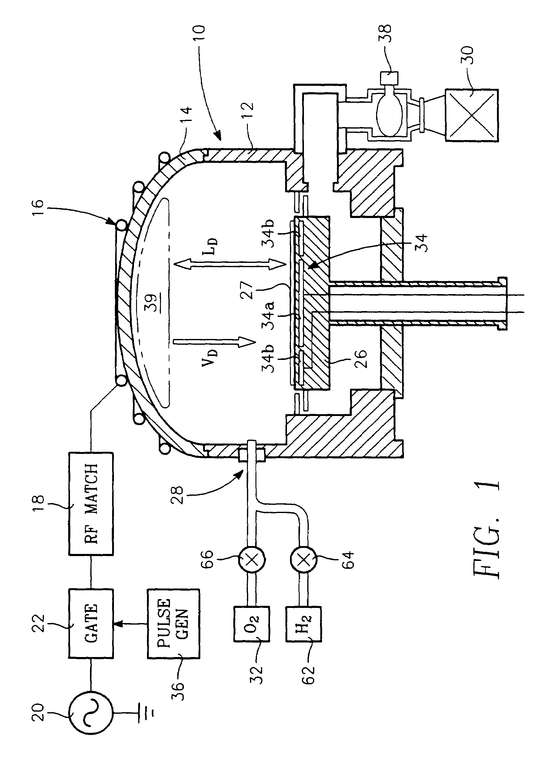
[0022]FIG. 1 illustrates a plasma reactor for carrying out the gate oxide formation process of the present invention. The reactor has an inductively coupled plasma source power applicator driven by a pulsed RF power generator. The reactor includes a chamber 10 having a cylindrical side wall 12 and a ceiling 14 which may be either dome-shaped (as shown in the drawing) or flat. The plasma source power applicator consists of a coil antenna 16 over the ceiling 14 coupled through an impedance match network 18 to an RF power source consisting of an RF power generator 20 and a gate 22 at the output of the generator 20 controlled by a pulse signal having a selected duty cycle. The reactor further includes a wafer support pedestal 26, which may be an electrostatic chuck, for holding a semiconductor wafer 27, a gas injection system 28 and a vacuum pump 30 coupled to the interior of the chamber. The gas injection system 28 is supplied by a process gas source, such as an oxygen container 32. Th...


PUM


Abstract

A method of fabricating a gate of a transistor device on a semiconductor substrate, includes the steps of placing the substrate in a vacuum chamber of a plasma reactor and introducing into the chamber a process gas that includes oxygen while maintaining a vacuum pressure in the chamber. An oxide insulating layer on the order of several Angstroms in thickness is formed at the surface of the substrate by generating a plasma in a plasma generation region within the vacuum chamber during successive “on” times, and allowing ion energy of the plasma to decay during successive “off” intervals separating the successive “on” intervals, the “on” and “off” intervals defining a controllable duty cycle. During formation of the oxide insulating layer, the duty cycle is limited so as to limit formation of ion bombardment-induced defects in the insulating layer, while the vacuum pressure is limited so as to limit formation of contamination-induced defects in the insulating layer. A conductive gate electrode is formed over the insulating layer.

Description

BACKGROUND OF THE INVENTION[0001]The present invention concerns the formation of a thin gate oxide beneath a gate electrode overlying a source-drain channel of a field effect transistor. The gate oxide is extremely thin (on the order of only Angstroms in thickness) and must be at least nearly free of defects in its amorphous silicon dioxide structure, such as dangling silicon or oxygen bonds. Such dangling bonds create quasi-mobile charge in the gate oxide, leading to two problems. One problem is that the electric fields associated with such charge perturb carrier motion in the source-drain channel, preventing a smooth current flow. Another problem is that such charge, to the extent it is mobile, may contribute to leakage between the gate electrode and the source-drain channel. Therefore, processes for forming the gate oxide must be free of any tendency to form defects in the gate oxide. Currently, only thermal oxide growth processes meet such criteria.[0002]Thermal processes for fo...

Claims


Application Information

Patent Timeline
Patent Type & Authority Patents(United States)
IPC IPC(8): H01L21/31H01L21/469
CPCH01J37/321H01L21/28167H01L21/28176H01L21/31683H01L21/02252H01L21/0223H01L21/205H01L21/31
Inventor CHUA, THAI CHENG
Owner APPLIED MATERIALS INC
Why Eureka
Try Eureka