Variable impedance circuit, variable gain differential amplifier, multiplier, high-frequency circuit and differential distributed amplifier

a technology of variable gain and amplifier, applied in the direction of electric/magnetic computing, instruments, computation using denominational number representation, etc., can solve the problems of small dynamic range, deterioration of distortion characteristics around a specific control voltage, and inferior power consumption and noise characteristics, so as to achieve the effect of stabilizing the operating current and simplifying the structure of each differential amplifier

Inactive Publication Date: 2007-05-08
SANYO ELECTRIC CO LTD
View PDF16 Cites 37 Cited by
  • Summary
  • Abstract
  • Description
  • Claims
  • Application Information

AI Technical Summary

Benefits of technology

[0028]An object of the present invention is to provide a variable impedance circuit capable of realizing reduced distortion without variation of an operating current, a variable gain differential amplifier using the same, and a multiplier using the same.
[0029]Another object of the present invention is to provide a variable impedance circuit capable of realizing reduced distortion while suppressing the saturation of input / output characteristics, a variable gain differential amplifier using the same, and a multiplier using the same.
[0030]Still another object of the present invention is to provide a high-frequency circuit in which a sufficiently increased dynamic range and reduced distortion is realized.

Problems solved by technology

An amplifier having the Gilbert-cell structure has a wide variable gain range, but is inferior in power consumption and noise characteristics.
In this case, the operating conditions of the Gilbert-cell multiplier are not optimized, resulting in a small dynamic range.
This causes deterioration in the distortion characteristics around a specific control voltage.
In the case of continuous gain control, therefore, the distortion characteristics of the variable gain differential amplifier are deteriorated when the FET is supplied with a control voltage at which waveform distortion is increased.
In addition, in a conventional receiver using the variable gain differential amplifier shown in FIG. 35, a sufficiently high dynamic range has not been realized.

Method used


Image

  • Variable impedance circuit, variable gain differential amplifier, multiplier, high-frequency circuit and differential distributed amplifier
  • Variable impedance circuit, variable gain differential amplifier, multiplier, high-frequency circuit and differential distributed amplifier
  • Variable impedance circuit, variable gain differential amplifier, multiplier, high-frequency circuit and differential distributed amplifier

Examples


first embodiment

[0131](First Embodiment)

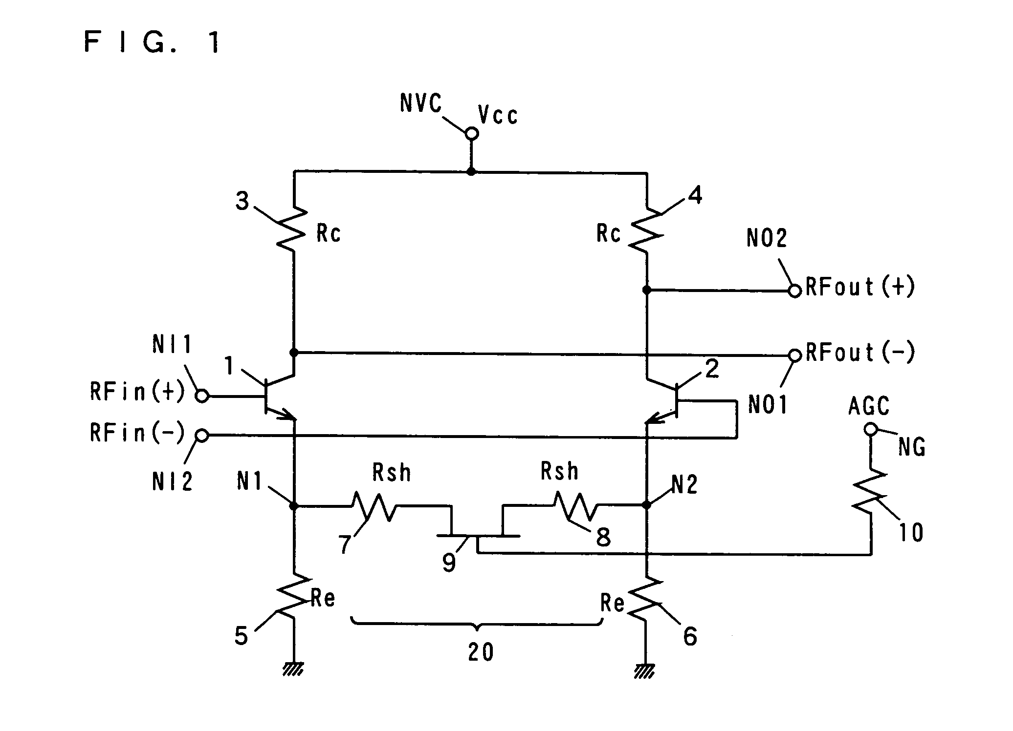
[0132]FIG. 1 is a circuit diagram showing the structure of a variable gain differential amplifier according to a first embodiment of the present invention.

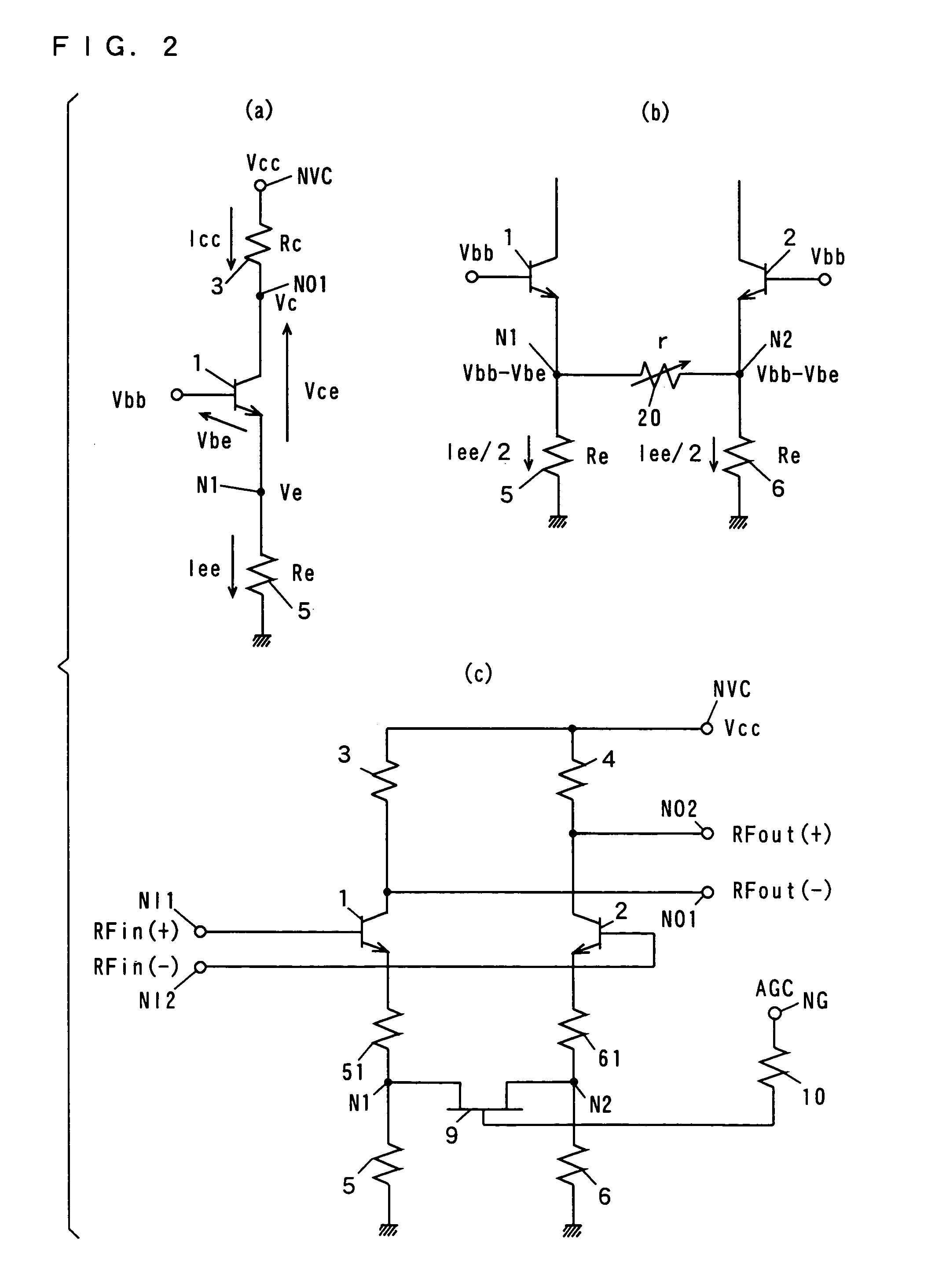
[0133]The variable gain differential amplifier shown in FIG. 1 comprises bipolar transistors (hereinafter abbreviated to transistors) 1, 2, resistances 3, 4, 5, 6, 10, shunt resistances 7, 8, and an n-MOSFET (hereinafter abbreviated to FET) 9. The shunt resistances 7, 8 form a variable resistance circuit 20. A bias voltage is determined by the resistances 3, 4, 5, 6.

[0134]The base of the transistor 1 is connected to an input terminal NI1 receiving an input signal RFin(+), and the base of the transistor 2 is connected to an input terminal NI2 receiving an input signal RFin(−). The input signals RFin(+) and RFin(−) are differential inputs. The collectors of the transistors 1, 2 are connected to a power supply terminal NVC receiving a power supply voltage VCC via the resistances 3, 4, respectively. The emitter...

second embodiment

[0148](Second Embodiment)

[0149]FIG. 3 is a circuit diagram showing the structure of a Gilbert-cell multiplier (mixer) according to a second embodiment of the present invention.

[0150]The Gilbert-cell multiplier shown in FIG. 3 comprises bipolar transistors (hereinafter abbreviated to transistors) 1, 2, 31, 32, 33, 34, resistances 3, 4, 5, 6, 10, shunt resistances 7, 8, and an n-MOSFET (hereinafter abbreviated to FET) 9. The shunt resistances 7, 8 and the FET 9 form a variable resistance circuit 20. A bias voltage is determined by the resistances 3, 4, 5, 6.

[0151]The base of the transistor 1 is connected to an input terminal NI1 receiving an input signal RFin(+), and the base of the transistor 2 is connected to an input terminal NI2 receiving an input signal RFin(−). The input signals RFin(+), RFin(−) are differential inputs. The transistors 31, 32 are inserted between the collector of the transistor 1 and an output terminal NO1 and between the collector of the transistor 1 and an out...

third embodiment

[0164](Third Embodiment)

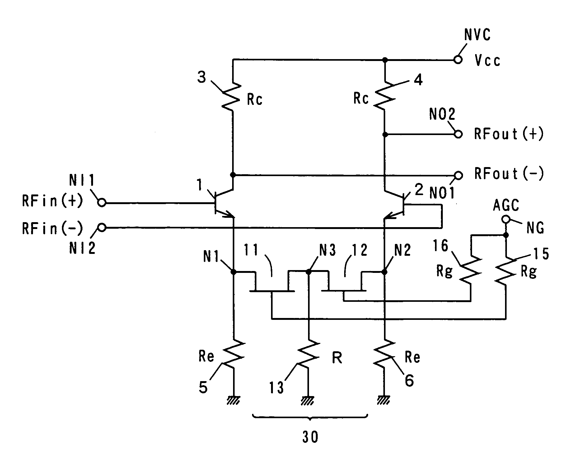
[0165]FIG. 6 is a circuit diagram showing the structure of a variable gain differential amplifier according to a third embodiment of the present invention.

[0166]The variable gain differential amplifier shown in FIG. 6 differs from the variable gain differential amplifier shown in FIG. 1 in that it is provided with a variable resistance circuit 30 in place of the variable resistance circuit 20.

[0167]The variable resistance circuit 30 comprises FETs 11, 12, and resistances 13, 15, 16. The FETs 11, 12 are connected in series between nodes N1 and N2. The gates of the FETs 11, 12 are connected to a control terminal NG receiving a control voltage AGC via the resistances 15, 16, respectively.

[0168]The resistances 3, 4 have an equal resistance value Rc; the resistances 5, 6 have an equal resistance value Re; and the resistances 15, 16 have an equal resistance value Rg.

[0169]Otherwise, the structure of the variable gain differential amplifier shown in FIG. 6 is the sa...


PUM


Abstract

The collectors of transistors are connected via respective resistances to a power supply terminal receiving a power supply voltage. The emitters of the transistors are connected to a ground terminal via respective resistances. A shunt resistance, a FET, and a shunt resistance are connected in series between nodes connected to the respective emitters of the transistors. The gate of the FET is connected via a resistance to a control terminal receiving a control voltage. The shunt resistances and FET form a variable resistance circuit.

Description

BACKGROUND OF THE INVENTION[0001]1. Field of the Invention[0002]The present invention relates to a variable impedance circuit, a variable gain differential amplifier using the same, a multiplier and a differential distributed amplifier using the same and a high-frequency circuit using them.[0003]2. Description of the Background Art[0004]Variable gain differential amplifiers (differential amplification circuits having a variable gain function) have been conventionally in use. Integrated circuits using Si (silicon) devices, such as bipolar transistors and MOSFETs (Metal Oxide Semiconductor Field-Effect Transistors), mainly include an amplifier having the Gilbert-cell structure or OTA (operational transconductance amplifier) structure as a variable gain differential amplifier.[0005]An amplifier having the Gilbert-cell structure has a wide variable gain range, but is inferior in power consumption and noise characteristics. For this reason, mobile communication devices and the like in ge...

Claims


Application Information

Patent Timeline
Patent Type & Authority Patents(United States)
IPC IPC(8): H03F3/45H03F1/56H03G3/10
CPCH03F3/45085H03F3/45098H03F3/45183H03F3/45197
Inventor BANBA, SEIICHINIKAI, NORIHIRO
Owner SANYO ELECTRIC CO LTD
Why Eureka
Try Eureka