Thin films for magnetic device

a thin film, magnetic device technology, applied in the direction of magnetic bodies, applications of chemical vapor deposition, instruments, etc., can solve the problems of device failure, sensitive to corrosion, and require very careful treatment, so as to avoid leakage current, reduce migration, and optimal thickness

Inactive Publication Date: 2007-05-22
ASM INTERNATIONAL
View PDF25 Cites 119 Cited by
  • Summary
  • Abstract
  • Description
  • Claims
  • Application Information

AI Technical Summary

Benefits of technology

[0015]These methods ensure near perfect uniformity in magnetic and non-magnetic conductors, and suppress migration that can cause spiking. In magnetic tunnel junction devices, dielectric layers of perfect uniformity allows optimal thickness, avoiding leakage current while keeping the layers thin enough to allow sensitivity for tunneling.

Problems solved by technology

There are problems associated with these techniques; pinholes, film thickness non-uniformity and impurities at the film interfaces have caused devices to fail.
In addition, ferromagnetic metals are rather sensitive to corrosion and thus require very careful treatment.
Unfortunately, CMP causes oxidation of some ferromagnetic materials.
), as high temperatures can destroy the functionality of the device.
Before this can happen, however, the remaining manufacturing problems of MRAM structures must be solved.
These can short-out the magnetic memory cell, rendering the device non-functional.
The MRAM layers are also temperature sensitive; defects can be expected if the layers are exposed to excessively high temperatures.

Method used


Image

  • Thin films for magnetic device
  • Thin films for magnetic device
  • Thin films for magnetic device

Examples


example 1

The Deposition of Aluminum Oxide by ALD

[0095]A substrate was loaded into a reactor configured for ALD processing. The reaction space was evacuated with a vacuum pump. After the evacuation, the pressure of the reaction space was adjusted to about 5–10 mbar (absolute) with flowing nitrogen gas that had a purity of 99.9999%. Then the reaction chamber was allowed to stabilize at 300° C. Alternating pulses of trimethyl aluminum (TMA) and water were introduced into the reaction space and made contact with the substrate surface. The reaction space was purged with nitrogen gas between the alternating pulses.

[0096]The growth rate of the amorphous Al2O3 film was 0.11 nm / cycle. The thickness variation of an aluminum oxide film was less than 1%. Advantageously, Al2O3 is thermodynamically stable and tends not to cause oxidation of the adjacent metal layers.

example 2

The Deposition of Copper Oxide by ALD and a Reducing Method

[0097]The deposition of copper oxide by ALD and its subsequent reduction to copper metal is described in Finnish patent application no. FI20001163, filed May 15, 2000, now abandoned, PCT application number FI01 / 00473, filed May 15, 2001 and U.S. patent application Ser. No. 09 / 975,466, filed Oct. 9, 2001, the disclosures of which are included herein by reference.

A. Reduction of CuO with Methanol Vapor

[0098]A substrate comprising a copper oxide layer is loaded into the reaction chamber of an Eagle 10™ reactor, commercially available from ASM Japan. The reaction chamber is evacuated to vacuum and heated to 360° C. The pressure of the reaction chamber is adjusted to about 5–10 mbar with flowing nitrogen gas.

[0099]Methanol vapor is mixed with nitrogen gas, introduced to the reaction chamber and contacted with the substrate.

[0100]Excess methanol and reaction by-products are purged from the reaction chamber by flowing nitrogen gas....

example 3

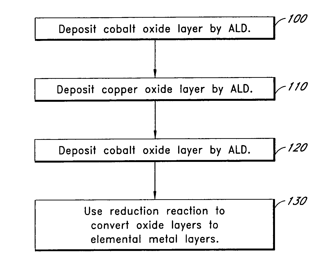
The Deposition of Cobalt Oxide by ALD and a Reducing Method

[0125]Cobalt oxide (CoO) was deposited by ALD from alternating pulses of Co(thd)3 and an ozone / oxygen mixture. A substrate was loaded into the reaction space of an ALD reactor. The reaction space was evacuated with a vacuum pump. The reaction space temperature was adjusted to 250° C. Cobalt source gas Co(thd)3 was heated to 110° C. in a source container inside the ALD reactor. Alternating pulses of cobalt source gas and the ozone / oxygen mixture were introduced into the reaction space. The ozone / oxygen mixture had a flow rate of about 100 std. cm3 / min during the ozone pulse.

[0126]The pulsing cycle consisted of the following steps:[0127]Co(thd)3 pulse 1.5 s[0128]N2 purge 2.0 s[0129]O3 pulse 3.0 s[0130]N2 purge 2.0 s.

[0131]The pulsing cycle was repeated 2000 times. The resulting thin film had a thickness of about 64 nm and a growth rate of about 0.03 nm / cycle. Stoichiometry of the CoO film was determined by energy dispersive x-...


PUM

PropertyMeasurementUnit
temperatureaaaaaaaaaa
thicknessaaaaaaaaaa
pressureaaaaaaaaaa

Abstract

Methods are provided for forming uniformly thin layers in magnetic devices. Atomic layer deposition (ALD) can produce layers that are uniformly thick on an atomic scale. Magnetic tunnel junction dielectrics, for example, can be provided with perfect uniformity in thickness of 4 monolayers or less. Furthermore, conductive layers, including magnetic and non-magnetic layers, can be provided by ALD without spiking and other non-uniformity problems. The disclosed methods include forming metal oxide layers by multiple cycles of ALD and subsequently reducing the oxides to metal. The oxides tend to maintain more stable interfaces during formation.

Description

RELATED APPLICATIONS[0001]The present application claims priority under 35 U.S.C. §119(e) to provisional application No. 60 / 250,533, filed Nov. 30, 2000.FIELD OF THE INVENTION[0002]This invention relates to magnetic structures for semiconductor devices and, more particularly, to a method for forming such structures by depositing thin films using atomic layer deposition (ALD). The magnetic structures may find use in magnetic random access memories (MRAMs) or in the magnetic field sensing elements that can be used in read-heads of computer hard-disk drives.BACKGROUND OF THE INVENTION[0003]Magnetic structures in integrated circuits and hard-disk read-heads include multi-layer devices comprising ferromagnetic films, conductive films and insulation films. These layered magnetic structures include magnetic tunneling junctions, spin-valve transistors and pseudo spin valves.[0004]Most commonly, physical vapor deposition (PVD) and chemical vapor deposition (CVD) processes are used for deposi...

Claims


Application Information

Patent Timeline
Patent Type & Authority Patents(United States)
IPC IPC(8): H01L21/4763G01R33/09C23C16/40G11B5/39H01F10/16H01F10/32H01F41/22H01F41/30H01F41/32H01L21/8246H01L27/105H01L27/22H01L29/82H01L43/08H01L43/12
CPCB82Y10/00B82Y25/00B82Y40/00G11B5/3909H01F10/3231H01F10/3254H01F41/22H01F41/307H01L43/12G11B5/3903G11B2005/3996H10N50/01G11C11/15
Inventor HUJANEN, JUHARAAIJMAKERS, IVO
Owner ASM INTERNATIONAL
Why Eureka
Try Eureka