Phase shifter device having a microstrip waveguide and shorting patch movable along a slot line waveguide

a phase shifter and microstrip technology, applied in waveguides, delay lines, antennas, etc., can solve the problems of low cost, low cost, relative phase shift between antenna elements, and the development of low cost adjustable phase shifters. achieve the effect of constant spacing of slot lines and microstrip waveguides and reduce noise levels

Inactive Publication Date: 2007-05-29
FLIR BELGIUM BVBA
View PDF8 Cites 17 Cited by
  • Summary
  • Abstract
  • Description
  • Claims
  • Application Information

AI Technical Summary

Benefits of technology

[0010]The present invention thus provides a convenient way of producing an adjustable phase shifter that can operate with low losses and is relatively cheap and simple to fabricate. In particular the provision of a moveable shorting patch in association with the micro-strip waveguide provides a transition that maximises transmission of radiation between the slot line and microstrip waveguides. This arrangement allows a controllable phase shift to be imparted to all the power contained in a signal, and is thus not restricted to the multiple way signal splitting phase shifter described in JP6326501. Furthermore, the requirement for a long length of meandering track as described in US2002 / 0003458 is removed.
[0014]Provision of a moveable first arm portion moveably mounted to the substrate provides a convenient means of carrying the microstrip waveguide. Furthermore, an arm portion formed from a dielectric material is advantageous, especially when the dielectric material is located between the substrate and the microstrip waveguide. This ensure a constant spacing of the slot line and microstrip waveguides.
[0015]Advantageously, the shorting patch is carried on a second arm portion that is moveably mounted to the substrate. Forming the arm portion from dielectric material is preferable, especially when the layer of dielectric material is located between the shorting patch and the substrate. This arrangement prevents metal to metal contact between the shorting patch and the slot line waveguide thereby reducing the level of noise typically associated with intermittent metal to metal contacts.
[0021]Preferably, the substrate comprises a layer of dielectric material and / or a layer of metal. The slot line waveguide may advantageously be formed by a layer of copper printed on to a dielectric substrate. The use of metal printing techniques (especially those utilizing copper metal) provide broad band waveguides at a low cost. Such techniques are highly suited to the fabrication of devices of the present invention.
[0024]According to a second aspect of the invention, a phase shifting array comprises a plurality of devices according to a first aspect of the invention. Building up such an array of phase shifters allows independently controllable phase shifts to be applied to the antenna elements of a phased array.
[0026]According to a fourth aspect of the invention, a phase shifting device comprises a substrate comprising a slot-line waveguide interfaced to a first radiation feed point, a first arm portion comprising a microstrip waveguide interfaced to a second radiation feed point and additionally arranged to intersect said slot-line waveguide at a first slot-line intersection point, and a second arm portion carrying a shorting patch arranged to short said slot-line at a second point of slot-line intersection, the first point of slot-line intersection being located on the slot-line waveguide between the first radiation feed point and the second point of slot-line intersection, and the second point of slot-line intersection being separated from the first point of slot-line intersection by a distance of slot-line waveguide substantially equal to one quarter of a wavelength of the radiation carried by the device, wherein the first and second arm portions are moveably mounted with respect to the substrate such that the location of the first and second points of slot-line intersection can be varied, whilst maintaining a substantially constant relative separation between the first and second points of slot-line intersection, thereby altering the path length between the first radiation feed point and the second radiation feed point.

Problems solved by technology

However, this fixes the relative phase shifts between the antenna elements which may be undesirable in certain applications where phase adjustment is required.
Although such an approach is highly suited to radar applications, the complexity and cost of the electronic circuitry is prohibitively expensive for low cost, mass market, applications.
In cases where rapid phase control is not required, but providing a fixed relative phase difference is insufficient, low complexity adjustable phase shifters have been developed.
A drawback of the device of US2002 / 0003458 is that the linear movement of the moveable dielectric element does not provide a correspondingly linear change in the phase shift imparted to the signal as the effect of the dielectric element is difficult to predict.
This can make it difficult to control the amount of phase shift imparted to a signal.
A disadvantage of the device of JP6326501 is that it is only possible to operate the device as a combined signal splitter and phase shifter.
Furthermore, independent control of the phase shift imparted to each of the four output signals is not possible; the geometry of the device dictates the phase shifts imparted to each of the four output signals for a given orientation of the rotatable arm.

Method used


Image

  • Phase shifter device having a microstrip waveguide and shorting patch movable along a slot line waveguide
  • Phase shifter device having a microstrip waveguide and shorting patch movable along a slot line waveguide
  • Phase shifter device having a microstrip waveguide and shorting patch movable along a slot line waveguide

Examples


Embodiment Construction

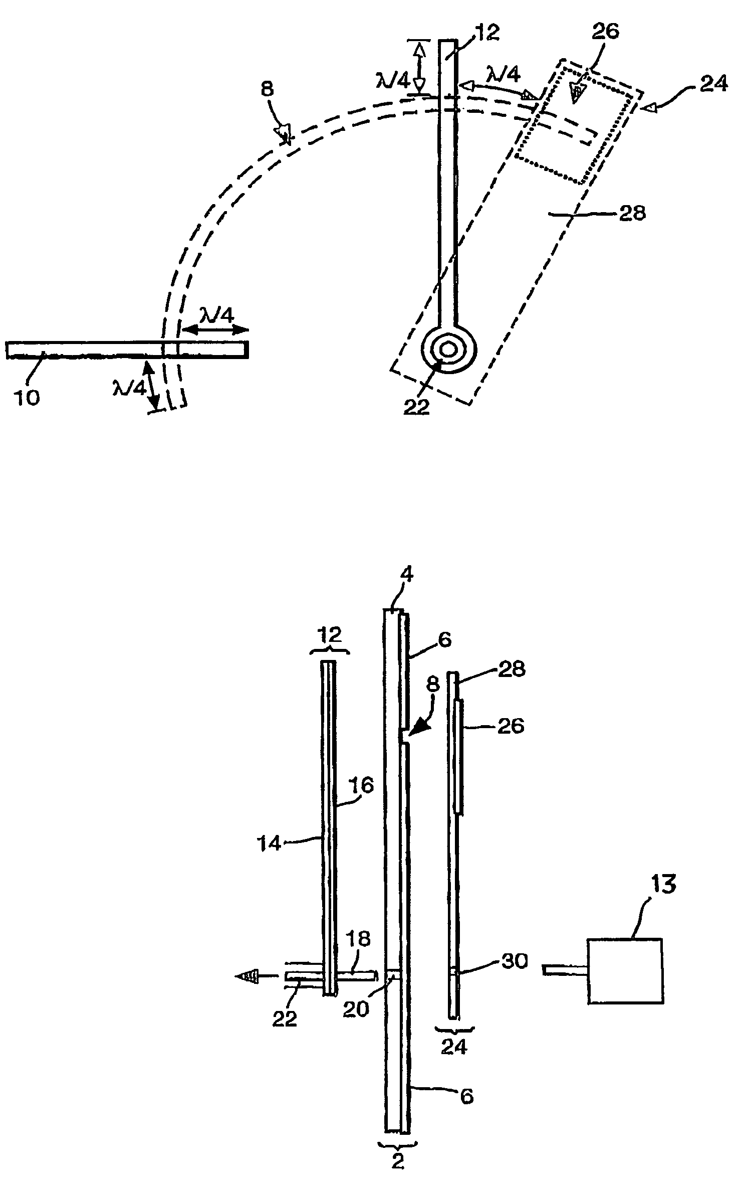
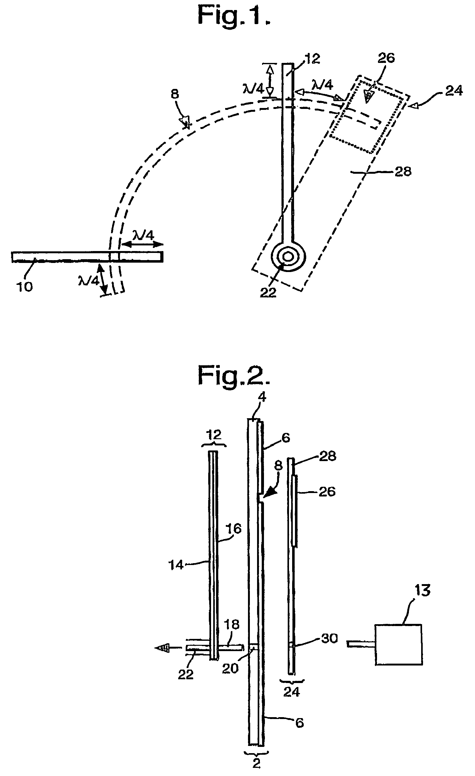
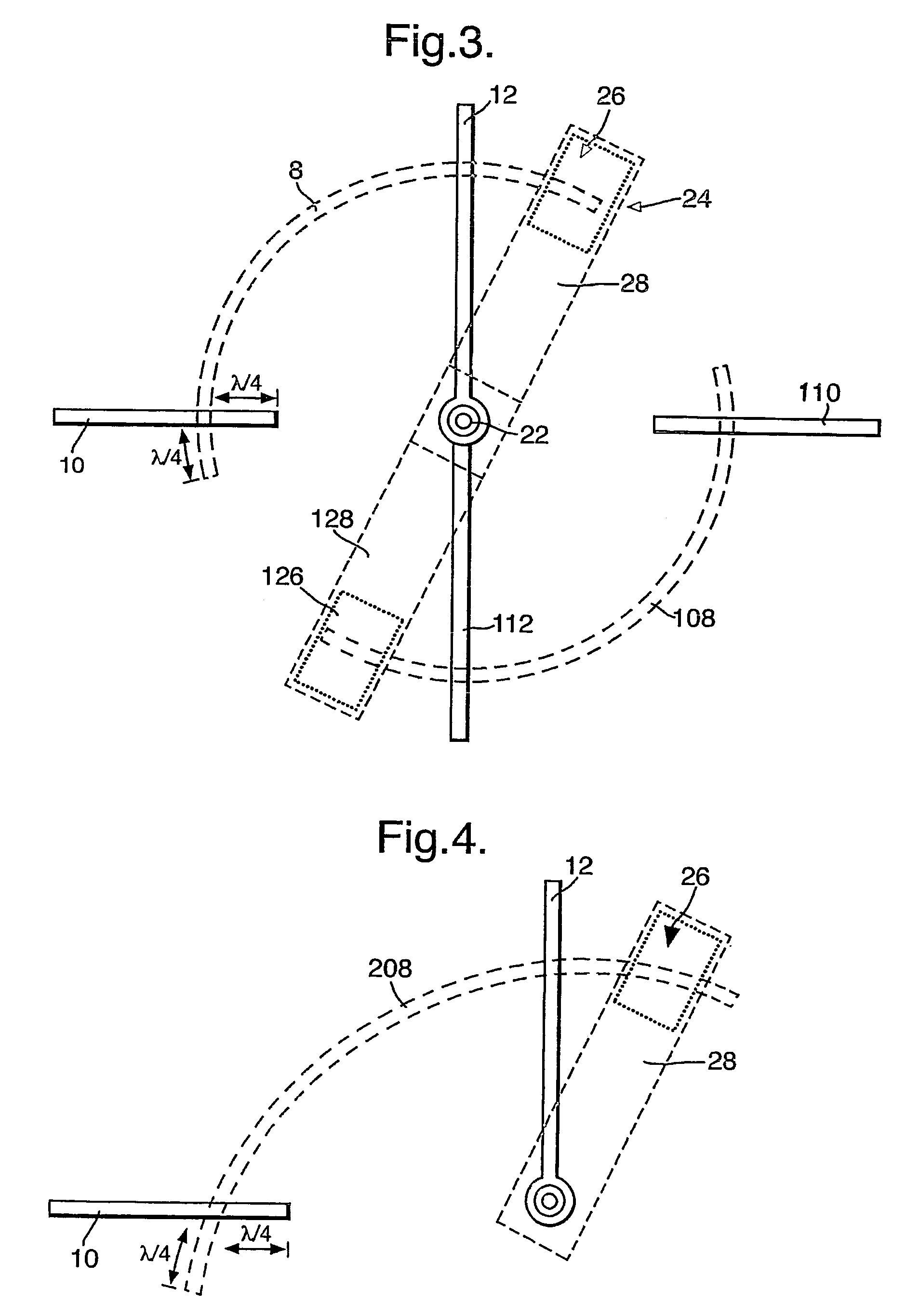
[0034]Referring to FIGS. 1 and 2, a schematic illustration of a phase shifter of the present invention is shown. The phase shifter comprises a substrate 2 formed from a dielectric layer 4 having a printed metal layer 6 (shown in FIG. 2) located on a first surface of thereof. A truncated circular slot line waveguide 8 is formed in the metal layer 6. An output microstrip waveguide 10 (not shown in FIG. 2) is provided at a first end of the slot line waveguide 8 on the second surface of the dielectric layer 4. A known micro-strip to slot line transition is provided to couple radiation to the input microstrip waveguide 10 from the slot line waveguide 8; the transition may comprise an microstrip to slot line interface or a shorting pin. The transition involves waveguides 8 and 10 crossing over each other with an overlap of distance λ / 4.

[0035]A first arm portion 12 is provided and comprises a microstrip waveguide 14 mounted on a thin layer of dielectric material 16 shown in FIG. 2. The lay...


PUM


Abstract

A phase shifter device comprising a substrate defining a slot line waveguide having first and second ends and being operably coupled to a microstrip waveguide and a shorting patch is described. The microstrip waveguide and shorting patch are moveable along the slot line waveguide so as to vary the distance between the first end of the slot line and the intersection of the slot line waveguide and microstrip waveguide whilst maintaining a substantially constant separation between the microstrip waveguide and the shorting patch. A separation between the microstrip waveguide and shorting patch equal to one quarter of the effective wavelength of the radiation carried by the device is described. The device is described for use in various phased array antenna systems.

Description

BACKGROUND OF THE INVENTION[0001](1) Field of the Invention[0002]This invention relates to a phase shifter device for use at microwave or radio frequencies, and more particularly to phased array antenna apparatus incorporating a plurality of such phase shifter devices.[0003](2) Description of the Art[0004]Phased array antennas are well known. In such devices the resultant radiation pattern transmitted (the transmit beam), or the radiation pattern received (the receive beam), is controlled by variation of the relative phase of the signal transmitted, or received, by each antenna element that forms the phased array. In this manner, it is possible to steer a transmit or receive beam electronically without any mechanical movement of the antenna.[0005]The phase differences necessary for phased array operation can be introduced in a variety of ways. One of the simplest techniques is to link each antenna element to a common feed point using co-axial cables of different length. However, thi...

Claims


Application Information

Patent Timeline
Patent Type & Authority Patents(United States)
IPC IPC(8): H01P1/18
CPCH01P1/184
Inventor DEAN, MICHAEL
Owner FLIR BELGIUM BVBA
Why Eureka
Try Eureka