Method of etching high aspect ratio features

a technology of high aspect ratio and feature, applied in the field of etch chemistries, can solve the problems of slow etching, effluent species being exhausted from the feature, and more difficult for etchant species to enter such deep etching holes, and achieve the effect of effective etching of high aspect ratio silicon features and sufficient strength

Inactive Publication Date: 2007-06-05
TOKYO ELECTRON LTD
View PDF21 Cites 18 Cited by
  • Summary
  • Abstract
  • Description
  • Claims
  • Application Information

AI Technical Summary

Problems solved by technology

These smaller top CDs make it more difficult for etchant species to enter such deeply etched holes during etching and for effluent species to be exhausted from the feature as it etches deeper into the silicon wafer.
This interaction results in much slower etching and therefore longer etch times, which in turn results in problems providing a mask that will survive the increasingly long etch times. Current technology is approaching a limit of the current masks to be effective with the current chemistry for deep trench etching.
However, several limitations have been cited for deep trench etch pertaining to the current etch chemistry.
For example, mask erosion, particularly near the feature entrance, has posed a formidable issue with current processes.
Additionally, mask erosion is attributed to physical sputtering by high energy ions, and decreasing SiO2 surface protection resulting from low silicon availability from smaller (high aspect ratio) features.
And lastly, current process chemistries are unable to control the upper profile and maintain an anisotropic etch with parallel side-walls.
The presence of HF in the processing plasma leads to an aggressive attack of the oxide mask.

Method used


Image

  • Method of etching high aspect ratio features
  • Method of etching high aspect ratio features
  • Method of etching high aspect ratio features

Examples


first embodiment

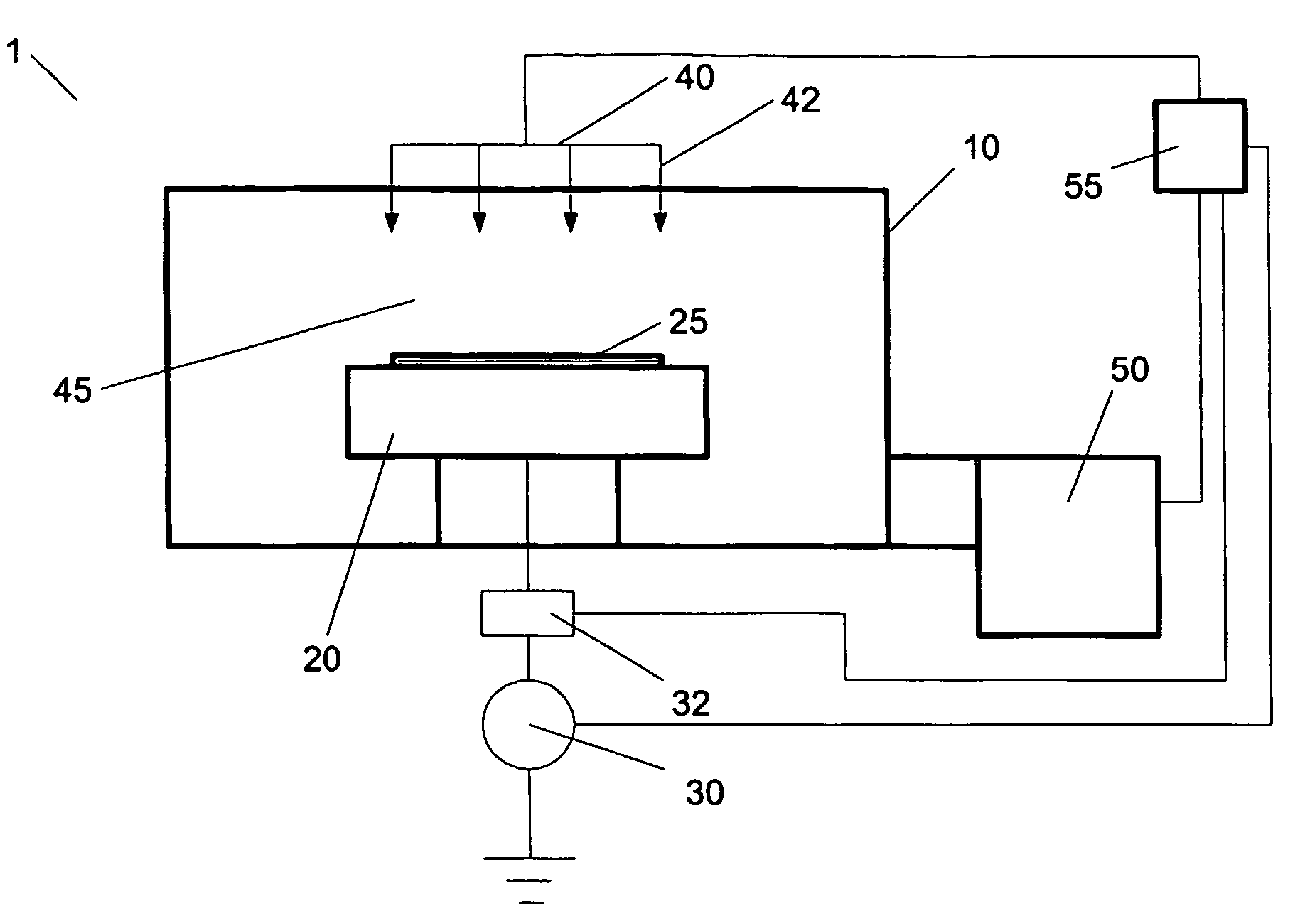
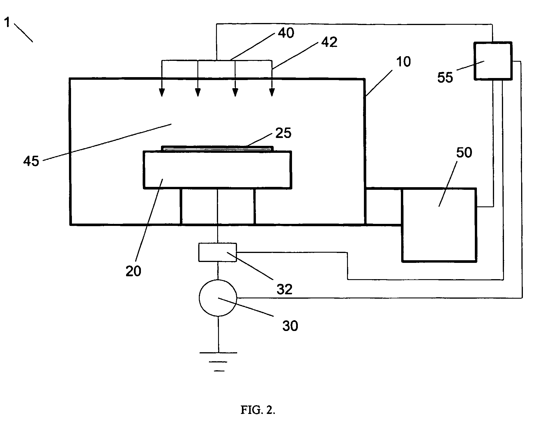
[0026]In a first embodiment, shown in FIG. 2, the substrate holder 20 further serves as an electrode through which radio frequency (RF) power is coupled to plasma in the processing region 45. For example, the substrate holder 20 is electrically biased at a RF voltage via the transmission of RF power from an RF generator 30 through an impedance match network 32 to the substrate holder 20. The RF bias serves to heat electrons and, thereby, form and maintain plasma. In this configuration, the system operates as a reactive ion etch (RIE) reactor, wherein the chamber and upper gas injection electrode serve as ground surfaces. A typical frequency for the RF bias ranges from 1 MHz to 100 MHz and is preferably 13.56 MHz.

[0027]In an alternate embodiment, RF power is applied to the substrate holder electrode at multiple frequencies. Furthermore, the impedance match network 32 serves to maximize the transfer of RF power to plasma in processing chamber 10 by minimizing the reflected power. Matc...

second embodiment

[0031]In a second embodiment, shown in FIG. 3, the plasma processing system 1 further includes either a mechanically or electrically rotating dc magnetic field system 60, in order to potentially increase plasma density and / or improve plasma processing uniformity, in addition to those components described with reference to FIG. 2. Moreover, the computer 55 is coupled to the rotating magnetic field system 60 in order to regulate the speed of rotation and field strength.

third embodiment

[0032]In a third embodiment, shown in FIG. 4, the plasma processing system 1 of FIG. 2 further includes an upper plate electrode 70 to which RF power is coupled from an RF generator 72 through an impedance match network 74. A typical frequency for the application of RF power to the upper electrode ranges from 10 MHz to 200 MHz and is preferably 60 MHz. Additionally, a typical frequency for the application of power to the lower electrode ranges from 0.1 MHz to 30 MHz and is preferably 2 MHz. Moreover, the computer 55 is coupled to the RF generator 72 and the impedance match network 74 in order to control the application of RF power to the upper electrode 70.


PUM

PropertyMeasurementUnit
depthsaaaaaaaaaa
depthsaaaaaaaaaa
feature aspect ratio L/daaaaaaaaaa

Abstract

A plasma processing system for and method of utilizing an improved etch chemistry for effectively etching high aspect ratio silicon features. The process chemistry employs precursor gases suitable for producing a fluorine / chlorine etch chemistry as well as precursor gases suitable for forming chemical bonds of sufficient strength to create stable feature side-walls. The improved process chemistries include SO2 / SF4 / SiCl4, SO2 / SF4 / Cl2, SO2 / SiF4 / SiCl4, SO2SIF4 / Cl2, O2 / F2 / Cl2, N2 O / F2 / Cl2, and NO2 / F2 / Cl2-based chemistries.

Description

CROSS-REFERENCE TO RELATED APPLICATIONS[0001]The present application claims priority to U.S. provisional Ser. No. 60 / 330,788, filed on Oct. 31, 2001, the entire contents of which are herein incorporated by reference.BACKGROUND OF THE INVENTION[0002]1. Field of Invention[0003]The present invention relates to etch chemistries and more particularly to a method for utilizing improved etch chemistries to etch high aspect ratio features.[0004]2. Discussion of the Background[0005]In the semiconductor industry there is a demand for increasing the speed of integrated circuits in general, and memory devices in particular. These demands force semiconductor manufacturers to make devices smaller and smaller on a surface of a semiconductor wafer. Accordingly, the increasingly small top critical dimensions (CDs) used to manufacture semiconductor chips require deep trench capacitors, which are used to store charge for memory, that must go deeper into the silicon to retain the same internal surface ...

Claims


Application Information

Patent Timeline
Patent Type & Authority Patents(United States)
IPC IPC(8): H01L21/302H01L21/00H01L21/3065
CPCH01J37/32082H01J37/3244H01L21/67069H01L21/3065H01J2237/3341
Inventor MOSDEN, AELANHYLAND, SANDRAKAJIMOTO, MINORI
Owner TOKYO ELECTRON LTD
Why Eureka
Try Eureka