Polysilicon conductor width measurement for 3-dimensional FETs

a polysilicon conductor and 3-dimensional fet technology, applied in the direction of semiconductor/solid-state device testing/measurement, semiconductor device details, semiconductor/solid-state device testing/measurement, etc., can solve the problem of gate oxide leakage through the gate oxide, the fet scaling is currently running into limits, and the gate oxide thin

Inactive Publication Date: 2007-06-05
IBM CORP
View PDF9 Cites 198 Cited by
  • Summary
  • Abstract
  • Description
  • Claims
  • Application Information

AI Technical Summary

Benefits of technology

[0018]The current invention teaches a test structure for easily determining the finished width of a polysilicon conductor (and therefore the FET channel length defined by the polysilicon conductor width) that serves as a gate electrode of a FinFET, a three dimensional field effect transistor. The finished width of a polysilicon conductor is the finished width of the polysilicon conductor after completion of processing the polysilicon conductor in a semiconductor process.
[0019]In an apparatus embodiment of the invention, two or more resistors are formed, each resistor having two contacts that allow resistive measurements to be taken. Each of the two or more resistors is routed over one or more semiconductor (typically silicon) “fins”, in a direction substantially orthogonal to the direction of the fins as viewed from the top. Each of the two or more resistors is constructed with one or more fingers of the polysilicon conductor. A first of the two or more resistors is designed with fingers of a first width of the polysilicon conductor. A second of the two or more resistors is designed with fingers of a second width, with a known, but slight, difference from the first width. In embodiments shown and described, a third resistor is implemented. The third resistor is designed with fingers of a third width, the third width slightly different from both the first width and the second width. Calculations made using measured resistance of each of the resistors determine the widths of the fingers in the resistors. Those skilled in the art will understand that table lookup or other suitable techniques could also be used, instead of a calculation, to determine the widths of the fingers, using the resistance of each of the resistors. Advantageously, the first width is designed to be equal to the nominal width of polysilicon conductors used to make FET gates on the semiconductor chip, therefore providing the value of the effective channel length for FETs on a particular chip made in a semiconductor process, since polysilicon conductor width is the primary determinant of the effective channel length of an FET. Those skilled in the art will recognize that although two resistors suffice to make a determination of the polysilicon conductor width, accuracy is improved by implementing more than two resistors.

Problems solved by technology

Scaling of FETs is currently running into limits.
Gate oxides have become thin enough that leakage occurs through the gate oxides.
Further scaling of gate oxide thickness will bring an exponential increase in leakage.
Power dissipated by leakage currents has become a significant portion of total chip power, and an exponential increase in leakage results in unacceptable power dissipation for many types of chips.
However, conventional SOI processes are reaching fundamental limits, resulting in undesirable effects such as the leakage effects mentioned above.
The nonuniform thickness of polysilicon gate 18 as it goes over the “fins” renders the prior art test structure and method described above relatively ineffective in determining a channel length of a FinFET.

Method used


Image

  • Polysilicon conductor width measurement for 3-dimensional FETs
  • Polysilicon conductor width measurement for 3-dimensional FETs
  • Polysilicon conductor width measurement for 3-dimensional FETs

Examples


Embodiment Construction

[0031]The invention will be described in detail with reference to the figures. It will be appreciated that this description and these figures are for illustrative purposes only, and are not intended to limit the scope of the invention. In particular, various descriptions and illustrations of the applicability, use, and advantages of the invention are exemplary only, and do not define the scope of the invention. Accordingly, all questions of scope must be resolved only from claims set forth elsewhere in this disclosure.

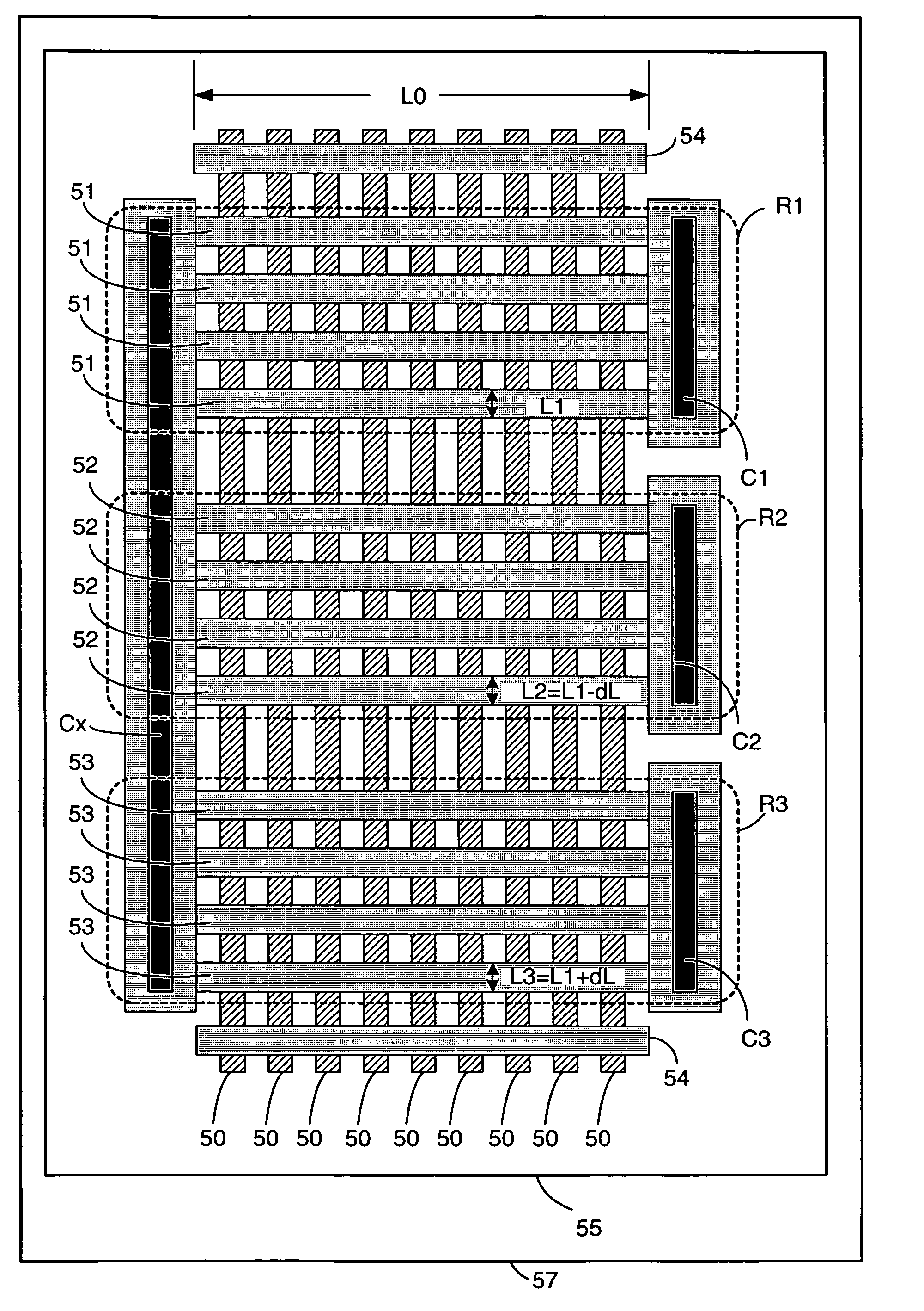
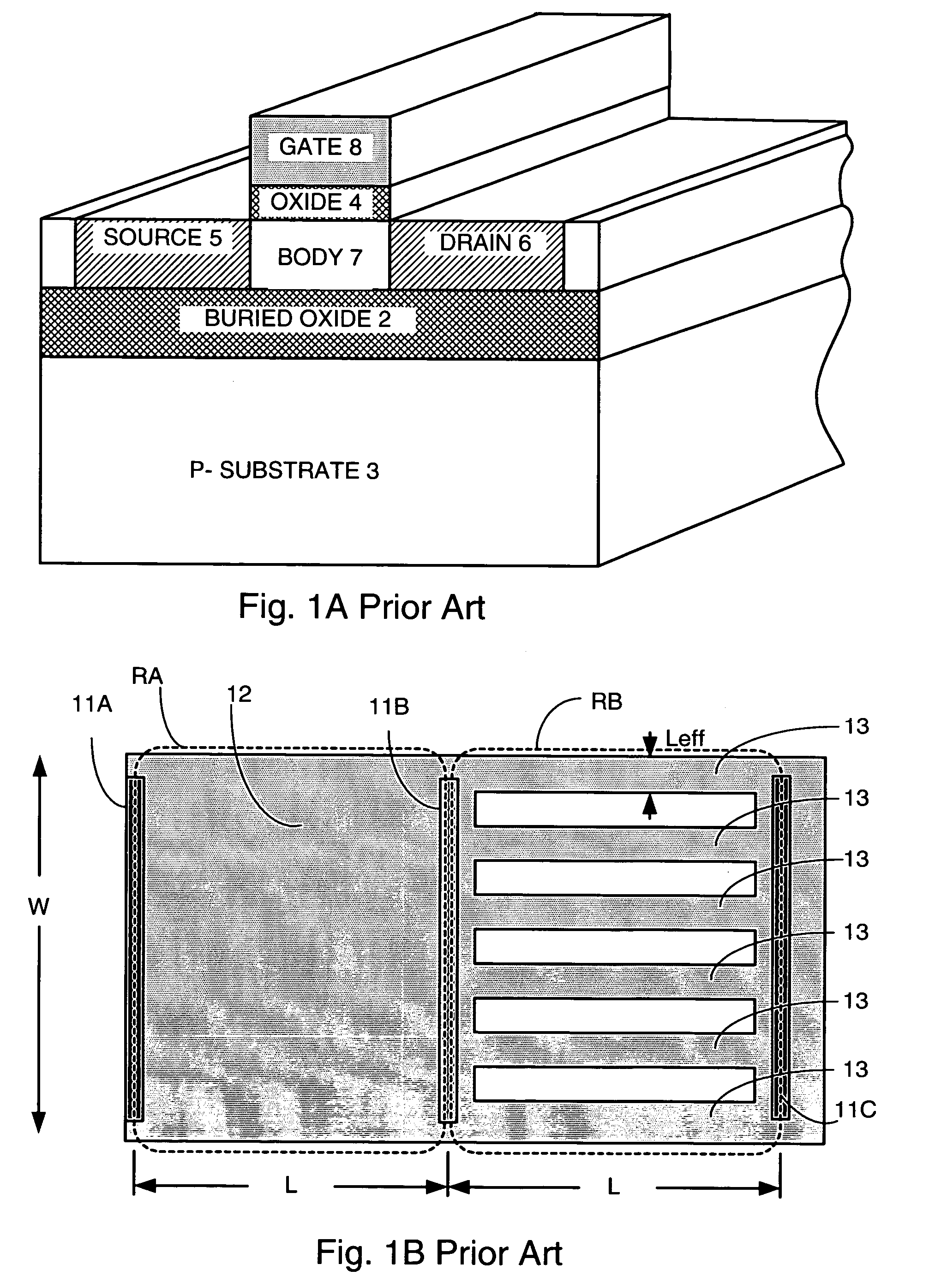
[0032]The current invention teaches a test structure apparatus that provides for easily determining a processed width of a polysilicon conductor that travels over one or more semiconductor “fins” on a FinFET semiconductor chip. A processed width is a final width of the polysilicon conductor after completion of a polysilicon etching step in a semiconductor process. The one or more semiconductor fins rise from a dielectric surface on the semiconductor chip. Although fins...


PUM


Abstract

An apparatus and method is disclosed for determining polysilicon conductor width for 3-dimensional field effect transistors (FinFETs). Two or more resistors are constructed using a topology in which polysilicon conductors are formed over a plurality of silicon “fins”. A first resistor has a first line width. A second resistor has a second line width. The second line width is slightly different than the first line width. Advantageously, the first line width is equal to the nominal design width used to make FET gates in the particular semiconductor technology. Resistance measurements of the resistors and subsequent calculations using the resistance measurements are used to determine the actual polysilicon conductor width produced by the semiconductor process. A composite test structure not only allows calculation of the polysilicon conductor width, but provides proof that differences in the widths used in the calculations do not introduce objectionable etching characteristics of the polysilicon conductors.

Description

BACKGROUND OF THE INVENTION[0001]1. Field of the Invention[0002]The current invention generally relates to semiconductor products. More specifically, the present invention relates to making electrical resistance measurements that allow accurate measurement of the width of polysilicon conductors used in making FET (field effect transistor) gates in a FinFET semiconductor process.[0003]2. Description of the Related Art[0004]Field Effect Transistors (FETs) have been the dominant semiconductor technology used to make Application Specific Integrated Circuit (ASIC) chips, microprocessor chips, Static Random Access Memory (SRAM) chips, and the like for many years. In particular, Complementary Metal Oxide Semiconductor (CMOS) technology has dominated the semiconductor process industry for a number of years.[0005]Technology advances have scaled FETs on semiconductor chips to increasingly small dimensions, allowing power per logic gate to be dramatically reduced, and further allowing a very l...

Claims


Application Information

Patent Timeline
Patent Type & Authority Patents(United States)
IPC IPC(8): H01L21/66
CPCH01L22/34H01L27/1203H01L29/785
Inventor DONZE, RICHARD LEEHOVIS, WILLIAM PAULKUEPER, TERRANCE WAYNESHEETS, II, JOHN EDWARDTETZLOFF, JON ROBERT
Owner IBM CORP
Why Eureka
Try Eureka