Feedback DAC chopper stabilization in a CT single-ended multi-bit sigma delta ADC

a multi-bit sigma delta, chopper technology, applied in analogue/digital conversion, transmission systems, instruments, etc., can solve the problems of deteriorating noise performance, increasing die cost, using a continuous-time front-end adc, etc., to reduce flicker noise

Active Publication Date: 2007-06-05
ANALOG DEVICES INC
View PDF16 Cites 12 Cited by
  • Summary
  • Abstract
  • Description
  • Claims
  • Application Information

AI Technical Summary

Benefits of technology

[0012]A multi-bit sigma-delta analog-to-digital converter (ADC), as set out in the appended claims, has a multi-bit feedback current digital-to-analog converter (IDAC) which generates a multi-level feedback current. An input signal is summed with the feedback current at a summing node. The IDAC is selectively connectable to the summing node via a first path and a second path. The first path transmits current from current sources within the IDAC to the summing node with a first polarity and the second path transmits current from the IDAC to the summing node with an inverted polarity. The provisioning of first and second paths which transmit current with opposite polarity can reduce flicker noise. The feedback signal is typically a multibit digital feedback signal derived from a Flash ADC at a downstream stage.
[0019]This arrangement can be used with bias current sources, which are preferably chopper stabilized, or without bias current sources. The provision of first and second paths to the summing node in this manner has an effect of balancing currents within the converter during a mid-scale (no input signal) condition and allows the biasing current sources to be removed. This further reduces flicker noise since the flicker noise that would have been contributed by the bias current sources is no longer present. Another benefit of this arrangement is that the total current through the switching portion of the IDAC is half that of the conventional single-ended IDAC circuit as show in FIG. 2. This is because all currents are used to cancel the incoming signal current whereas conventionally only half of the current sources are used when operating at mid-scale.
[0020]Preferably, amplifiers used within the first stage of the ADC are chopper-stabilized. Advantageously, each amplifier uses two gain stages, a first gain stage with a differential input and differential output and a second gain stage having a differential input and single-ended output, with only the first gain stage being chopper-stabilized. The gain of the first stage integrator makes the flicker noise in the amplifiers of successive integrator stages negligible.

Problems solved by technology

However, relatively large signal ranges, e.g. 2 Vrms, used for television audio are outside the voltage range that switched-capacitor based circuits implemented in deep sub-micron process technologies can easily interface to.
OEMs typically demand that this functionality is provided on-chip, inevitably leading to an increased die cost along with deteriorated noise performance.
However, there remain problems in using a continuous-time front-end ΣΔ ADC.
The circuit shown in FIG. 2 has certain disadvantages, including: (1) common-mode noise is not rejected in this single-ended input structure; (2) even harmonics produced in the IDAC are not cancelled; (3) chopping the IDAC current sources, as well as the DC biasing current source flicker noise, is not possible in this single-ended input structure.

Method used


Image

  • Feedback DAC chopper stabilization in a CT single-ended multi-bit sigma delta ADC
  • Feedback DAC chopper stabilization in a CT single-ended multi-bit sigma delta ADC
  • Feedback DAC chopper stabilization in a CT single-ended multi-bit sigma delta ADC

Examples


first embodiment

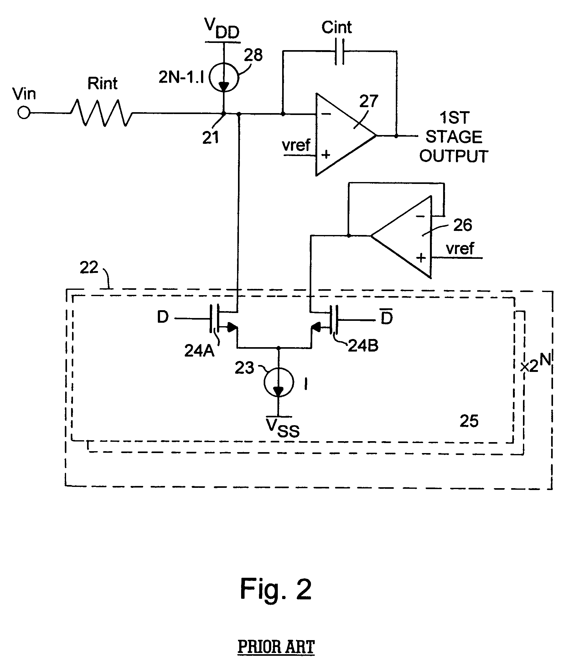
[0038]A front-end of an ADC according to the invention is shown in FIG. 4. This corresponds to stage 15 of FIG. 3. The front-end has a single-ended input Vin and a single-ended output 80. Typically, an input signal will connect to Vin via a dc decoupling capacitor (not shown). The front-end comprises two DC biasing current sources 31, 32 which each supply a bias current of value 2N−2.I, where N is the number of bits used for the multi-bit feedback signal. A first biasing current source 31 is connected between a supply rail VDD and a summing node 41 via chopping switches 35. A second biasing current source 32 is connected between the supply rail VDD and a node 42 via chopping switches 35. A multi-bit current digital-to-analog converter (IDAC) 50 is connected to the nodes 41, 42. The IDAC comprises a set of 2N unit IDACs, one of which is shown as 55 in FIG. 4. The IDAC 50 receives a multi-bit (i.e. N-bit) digital feedback signal which is used to select a number of the unit value IDACs...

second embodiment

[0046]A front-end according to the invention is shown in FIG. 6. In this embodiment the biasing current sources 31, 32 and chopping switches 35 of FIG. 4 are removed. The other components are the same as shown in FIG. 4 and similar numbering is used. The inclusion of the amplifier 60 and resistor 64, which together form a current-to-voltage converter, along with the extra resistor 65 ensures that the IDAC produces a net zero current flowing into the summing junction 41 during mid-scale range. By removing the DC biasing current source, there is a benefit of an improved noise performance as the DC biasing current sources no longer contribute noise.

[0047]To illustrate operation of this arrangement, assume a mid-range (no input signal) condition where a 16 bit thermometer coded signal from the scrambler comprises 8 bits set high and 8 bits set low. This signal is applied to the 16 IDACs 50. This will set eight of the IDACs 50 to have D enabled high. This causes current sources 53 of tho...


PUM


Abstract

A multi-bit sigma-delta analog-to-digital converter (ADC) has a single-ended input for receiving an analog input signal. A multi-bit feedback current digital-to-analog converter (IDAC) generates a multi-level feedback current depending on a multibit digital feedback signal from a Flash ADC. The feedback current is summed with the input signal with the feedback current. The summed signal is integrated on a continuous-time basis. The IDAC is selectively connectable to the summing node via a first path and a second path. The first path transmits current from the IDAC to the summing node with a first polarity and the second path transmits current from the IDAC to the summing node with an inverted polarity. This can reduce flicker noise and can allow the converter to operate without any mid-scale biasing current sources.

Description

[0001]This application claims benefit of U. S. Provisional Application No, 60 / 650,359, filed on Feb. 4, 2005 and also claims benefit of U. S. Provisional Application No. 60 / 608,993, filed on Sep. 10, 2004.FIELD OF THE INVENTION[0002]This invention relates to multi-bit sigma delta analog-to-digital converters.BACKGROUND TO THE INVENTION[0003]Continuous-time (CT) Sigma Delta (ΣΔ) analog-to-digital converters (ADC) have received much attention in the last couple of years for applications that require signal bandwidths of several MHz. Continuous-time ADCs are more favourable over switched-capacitor ADCs due to their lower power requirements. Other advantages include better noise immunity due to their inherent anti-aliasing properties, which is especially advantageous in RF receivers. Also, the technology trend towards very deep submicron processes dictates lower power supply voltages. As a consequence, switched capacitor based circuits require boot-strapping techniques to drive the swit...

Claims


Application Information

Patent Timeline
Patent Type & Authority Patents(United States)
IPC IPC(8): H03M3/00
CPCH03M3/34H03M3/424H03M3/454
Inventor DEL MAR CHAMARRO MARTI, MARIAMORROW, PAUL JOHN
Owner ANALOG DEVICES INC
Why Eureka
Try Eureka