Look-ahead decision feedback equalizing receiver

a receiver and feedback technology, applied in the field of i/o interface, can solve the problems of data size margin, insufficient setup/hold time of the receiver circuit, limited data transmission rate, etc., and achieve the effect of high-speed data transmission

Inactive Publication Date: 2007-06-12
POSTECH ACAD IND FOUND
View PDF5 Cites 10 Cited by
  • Summary
  • Abstract
  • Description
  • Claims
  • Application Information

AI Technical Summary

Benefits of technology

[0016]It is, therefore, a primary object of the present invention to provide an equalizing receiver, which adopts a look-ahead decision feedback equalizing scheme, for compensating an attenuation of a high-frequency component of a signal and further over-sampling the compensated signal so that a skew between data and a clock is compensated, thereby facilitating a high speed data transmission.

Problems solved by technology

However, in such communications, the data transmission rate is limited by time jitter occurring in a PLL(phase locked loop) / DLL(delay locked loop) circuit, an offset due to dimensional deviations in the process of producing transmitters and receivers and so on.
Also a setup / hold time of a receiver circuit is not long enough, due to a reduction in a data size margin and a time margin resulting from an inter-symbol interference (ISI) between signals.
Moreover, a time skew is generated, due to a difference in time required for transmitting a signal through a channel, between signals or between a clock and the signal.
However, since a SSTL (series stub terminated logic) channel for a DRAM interface employs a full-swing voltage-mode driving technique at a transmitter output, it is difficult to use the pre-emphasis scheme for the SSTL channel.
In this way, noise immunity of the receiver may be degraded due to the analog nature of the signal and an equalization circuit cannot be simplified due to the presence of analog storage circuits, e.g., capacitors.
However, the DFE scheme has a limitation in a high-speed transmission due to a delay time at its feedback path.
Furthermore, due to a difference in time required for transmitting signals through channels, there is a time skew between transmitted signals or between a clock and a transmitted signal.
The skew has an adverse effect on signal transmission at a high speed.
For the normal operation of an input circuit in a receiver, a setup / hold time should be sufficient as needed, but the time skew makes it difficult.
That is, if a high-frequency component of the signal is considerably attenuated while passing through a transmission channel, the time uncertainty region of data is broadened, and the scheme for determining the suitability of the clock by using the over-sampling becomes ineffective due to an increase in time jitter.
Thus, the 2× over-sampling scheme cannot be used in a channel where a high-frequency component of a signal is seriously attenuated.
In transmitting a signal in the above-mentioned digital system, therefore, there may occur various problems as further explained below.
Such a phenomenon causes an ISI between signals and reduces a time margin and a voltage margin of the signal, thereby making it difficult to carry out data transmission at a high speed.
However, the equalizing technology applied to the terminal of the transmitter is not applicable to a DRAM or an ASIC where a voltage at the terminal of the transmitter has a waveform of a full swing.
Further, the equalizing technology applied to the terminal of the receiver has drawbacks such as low noise immunity and low-speed of data transmission.
Thirdly, when a clock signal is transmitted with a data signal from a transmitter to a receiver, a time skew is generated due to a difference in the delay time required for signals to pass through a transmission channel, which may in turn reduce the time margin of the data signal.
However, in the occurrence of an attenuation of a signal, it is very difficult to apply such a scheme to a broadened time uncertainty region of the data signal.

Method used


Image

  • Look-ahead decision feedback equalizing receiver
  • Look-ahead decision feedback equalizing receiver
  • Look-ahead decision feedback equalizing receiver

Examples


Embodiment Construction

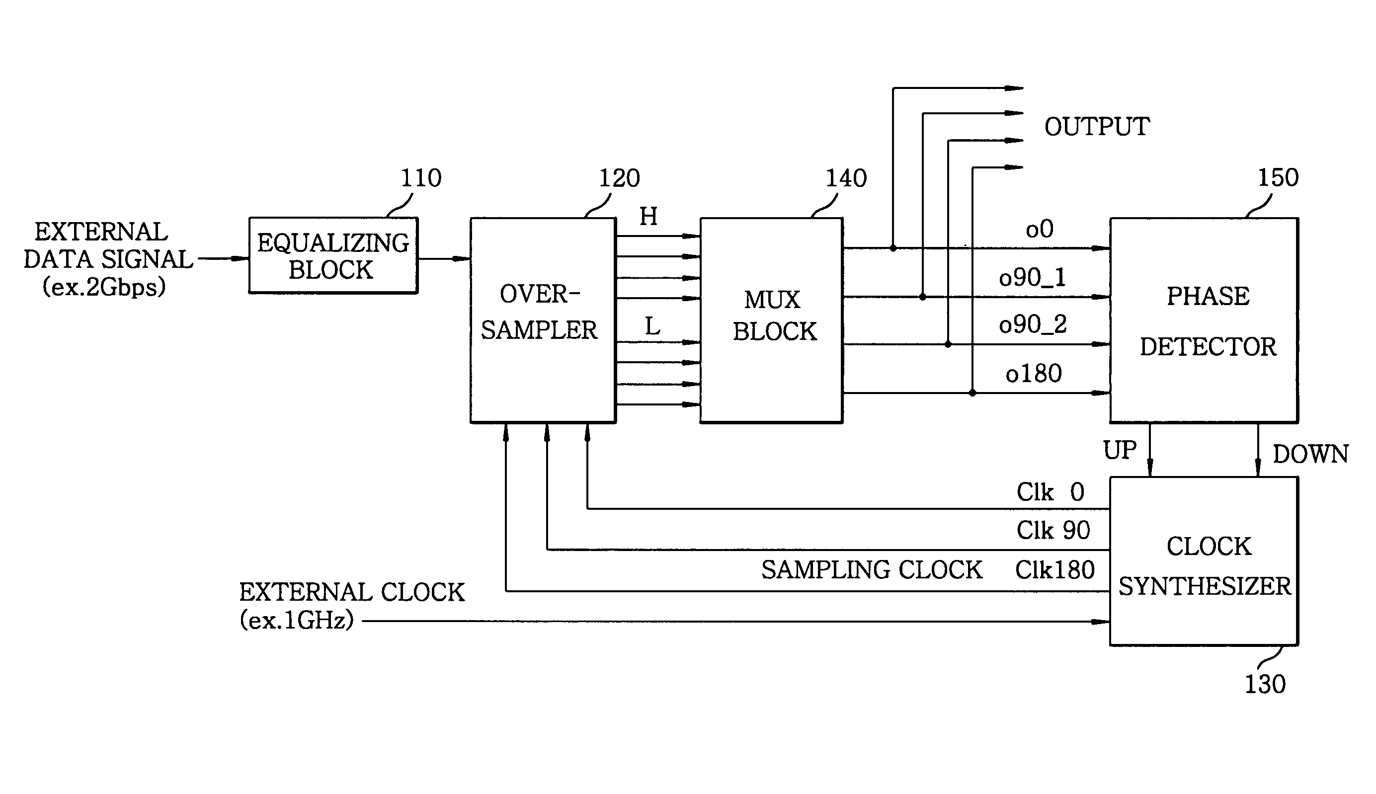
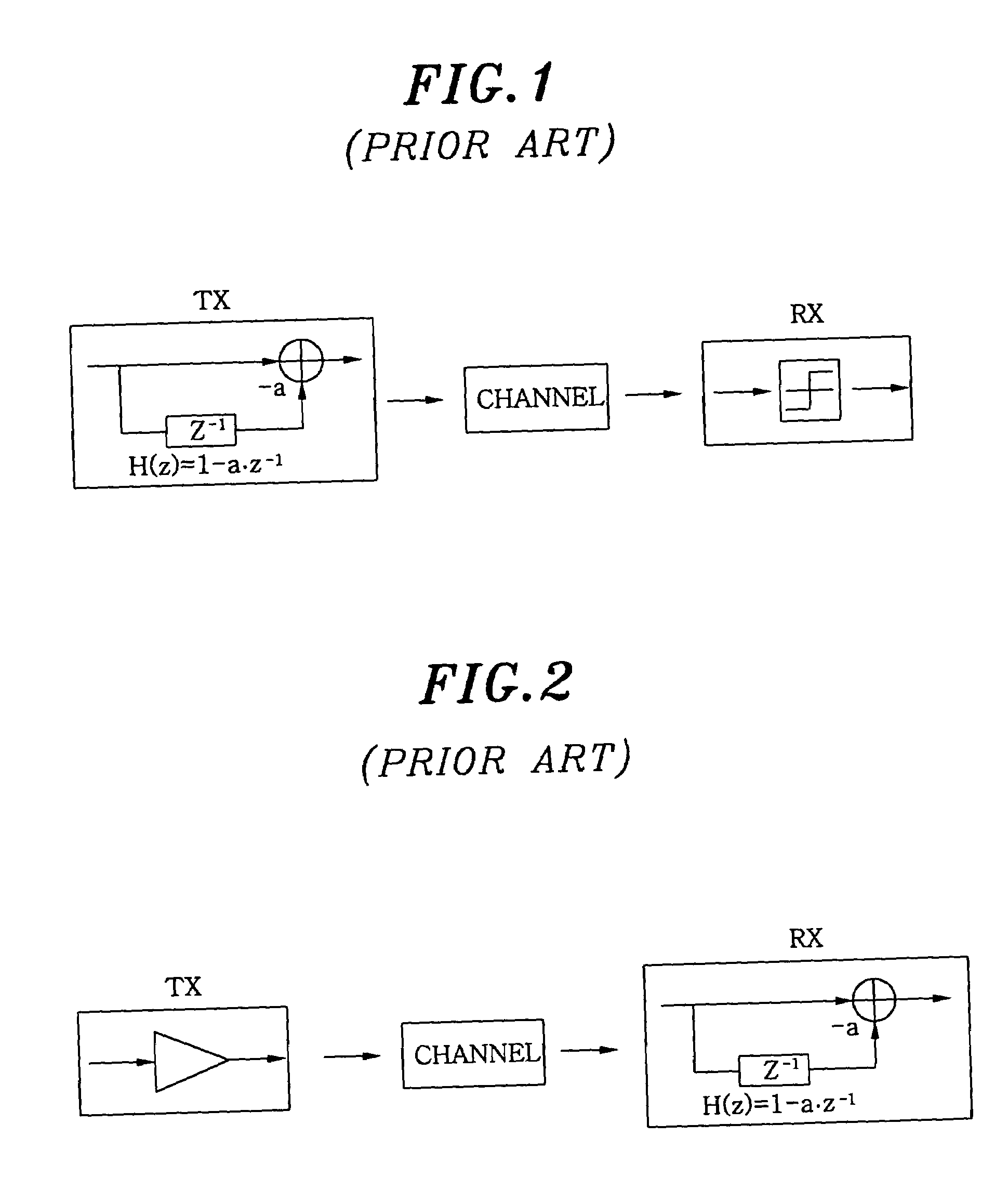
[0027]FIG. 5 is a block diagram illustrating a CMOS (complementary metal oxide semiconductor) receiver using a look-ahead decision feedback equalizing scheme in accordance with a preferred embodiment of the present invention. An external data signal with an attenuated high-frequency component is fed to an equalizing block 110 and an external clock signal synchronized with the external data signal is fed to a clock synthesizer 130. Herein, in case a DDR (double data rate) technology is applied to the receiver, the data transmission rates of the external data signal and the external clock signal are 2 Gbps and 1 GHz, respectively.

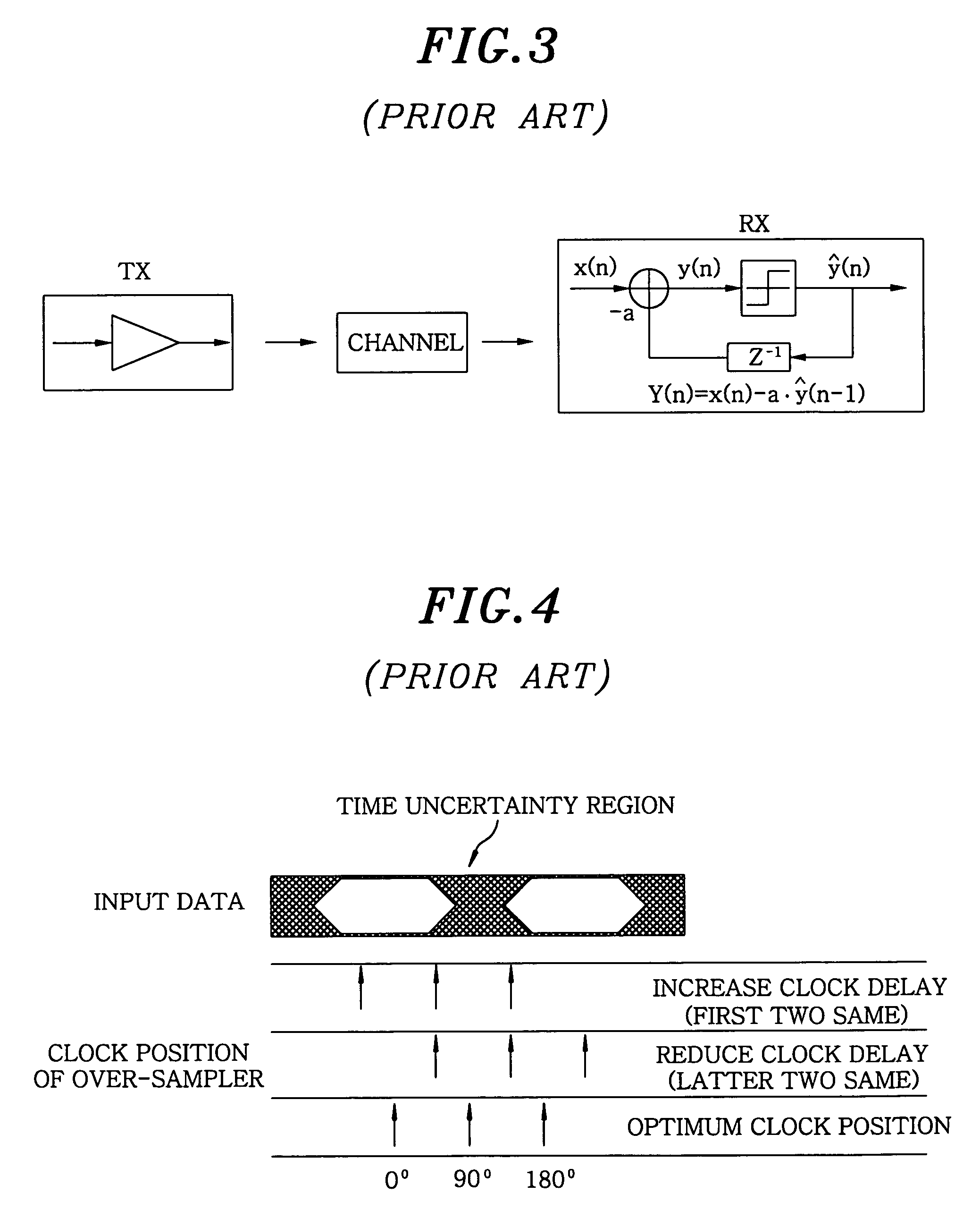
[0028]The equalizing block 110 equalizes the external data signals and provides the equalized signals to an over-sampler 120 which takes samples of the equalized external data signals at 0, 90° and 180° phase sampling clocks provided by the clock synthesizer 130 (See FIG. 4 and clk0, clk90, clk180 in FIG. 5).

[0029]Then, the outputs of the over-sampler 120 are...


PUM


Abstract

A look-ahead decision feedback equalizing receiver includes an equalizing block for amplifying a high-frequency component of an external data signal fed thereto in response to a first and a second input signal, to provide a first and a second equalized external data signal; a clock synthesizer for outputting sampling clocks, a timing thereof being adjusted by receiving an external clock synchronized with the external data signal; an over-sampler for over-sampling the first and the second equalized external data signal in synchronization with the sampling clocks. A MUX block for multiplexing the outputs of the over-sampler in response to outputs of the MUX block, to thereby attain decision results; and a phase detector for deciding the timing of the sampling clock by analyzing the decision results.

Description

FIELD OF THE INVENTION[0001]The present invention relates to an I / O interface for use in communications between an SDRAM (synchronous dynamic random access memory) and a controller or between digital chips; and, more particularly, to an equalizing receiver which employs a look-ahead decision feedback equalizing technology.BACKGROUND OF THE INVENTION[0002]The amount of data transmission as well as transmission rate of the data in communications between a DRAM(dynamic random access memory) and a CPU(central processing unit) or between digital chips such as ASICs(application specific integrated circuits) continue to rise.[0003]However, in such communications, the data transmission rate is limited by time jitter occurring in a PLL(phase locked loop) / DLL(delay locked loop) circuit, an offset due to dimensional deviations in the process of producing transmitters and receivers and so on. Also a setup / hold time of a receiver circuit is not long enough, due to a reduction in a data size marg...

Claims


Application Information

Patent Timeline
Patent Type & Authority Patents(United States)
IPC IPC(8): H03K5/159H04L27/00H03H7/30H03H7/40
CPCH04L25/03878H04L27/00
Inventor PARK, HONG-JUNESOHN, YOUNG-SOO
Owner POSTECH ACAD IND FOUND
Why Eureka
Try Eureka