Method of manufacturing an anisotropic conductive film

a technology of anisotropic conductive film and production method, which is applied in the direction of conductors, magnetic bodies, coupling device connections, etc., can solve the problems of preventing sufficiently high adhesion to an object, reducing the practicability of the step, and reducing the cost of the necessary step. , to achieve the effect of widening the interval

Inactive Publication Date: 2007-06-19
NITTO DENKO CORP
View PDF27 Cites 2 Cited by
  • Summary
  • Abstract
  • Description
  • Claims
  • Application Information

AI Technical Summary

Benefits of technology

[0007]It is therefore an object of the present invention to provide a production method of an anisotropic conductive film, which is capable of sufficiently widening the interval (pitch) of the centers of conductive paths without forming unnecessary voids in the film.
[0008]It is also an object of the present invention to provide an anisotropic conductive film, which has a sufficient strength and deformability, which shows fine follow-up property to an object to be connected, which is capable of connecting a conductive path to a terminal (electrode) of a test object with a low pressure, when used for testing connectors, and which can form a highly reliable electrical connection by firmly adhering to an object to be connected, when used as a mounting material.
[0009]It has been also found that an anisotropic conductive film free of unnecessary voids in the film, having a sufficiently large pitch of conductive paths (metal conductors), and having a decreased density of the conductive paths can be obtained by forming a laminate comprising alternate layers of a winding layer comprising a single row of insulated wires, and an insulating resin film, which laminate being made by placing an insulating resin film on the winding layer comprising the insulated wire wound around a core member, and cutting this laminate to give a film.

Problems solved by technology

However, this anisotropic conductive film is subject to restriction because a fine pitch connection is difficult to achieve and a convex terminal (e.g., bump contact) is required as a connection terminal of a semiconductor element.
However, a close study of the physical properties and the connection state of the connection mate of the anisotropic conductive film proposed above has revealed that the conductive path (metal conductor) in the film has a density higher than necessary, making the film hard to deform, which in turn tends to lower the follow-up property of the film to the connection target (particularly in the case of testing connectors, the degraded follow-up property of the film to the test target sometimes necessitates hard pressing of the film with a high pressure to bring a conductive path in contact with a terminal (electrode) of the test target), and that the density of the conductive path (metal conductor), which is higher than necessary, makes the amount of the insulating resin insufficient to provide an adhesive property when used as a material for mounting, thereby preventing sufficiently high adhesion to an object to be connected.
While the coating layer can be made thick by repeat coating the metal conductor wires with an insulating resin, the cost necessary for this step is not small at all and the step is impractical.
In addition, it is not that the thickness of the coating layer can be increased to any desired level, and the interval of the metal conductor wires (conductive paths) cannot be widened sufficiently.
In this case, however, unnecessary voids are formed between the metal conductor wires in the film, thus lowering the strength of the film to the extent that it is not practicable.

Method used


Image

  • Method of manufacturing an anisotropic conductive film
  • Method of manufacturing an anisotropic conductive film
  • Method of manufacturing an anisotropic conductive film

Examples


example 1

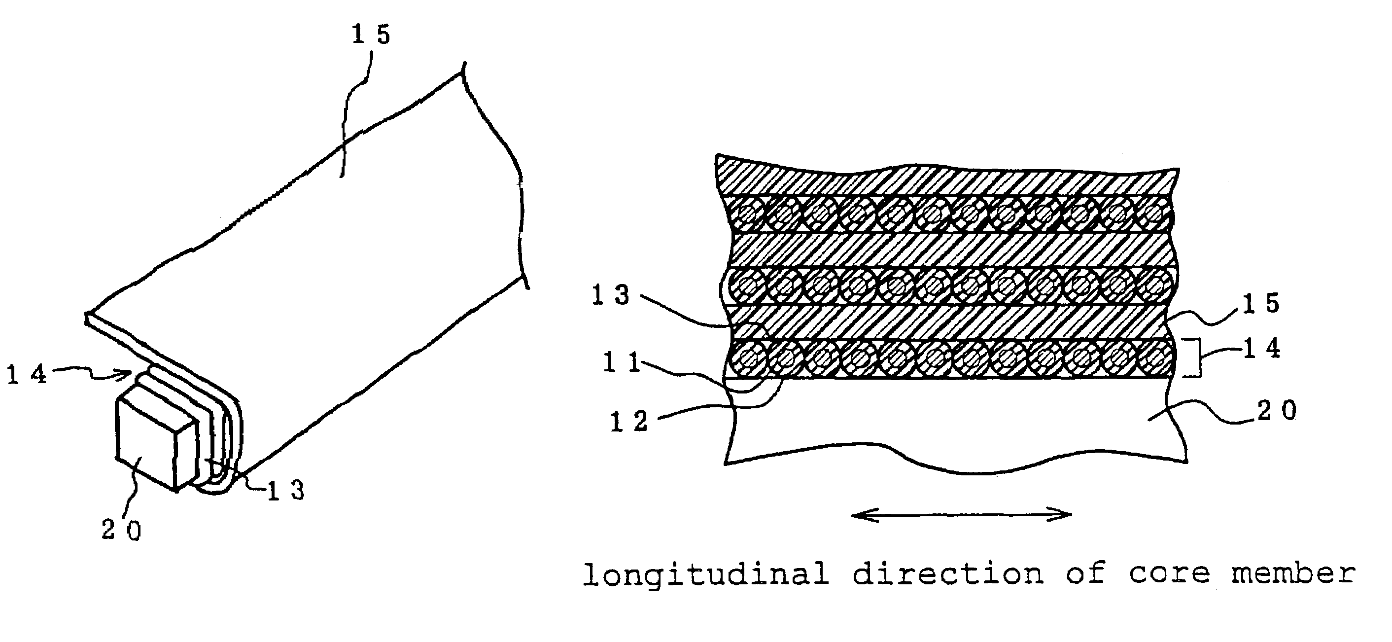
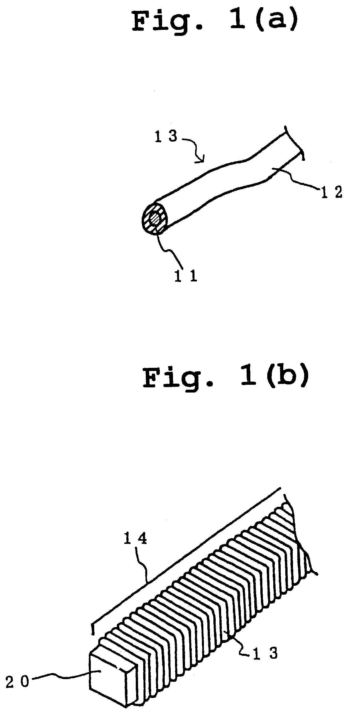
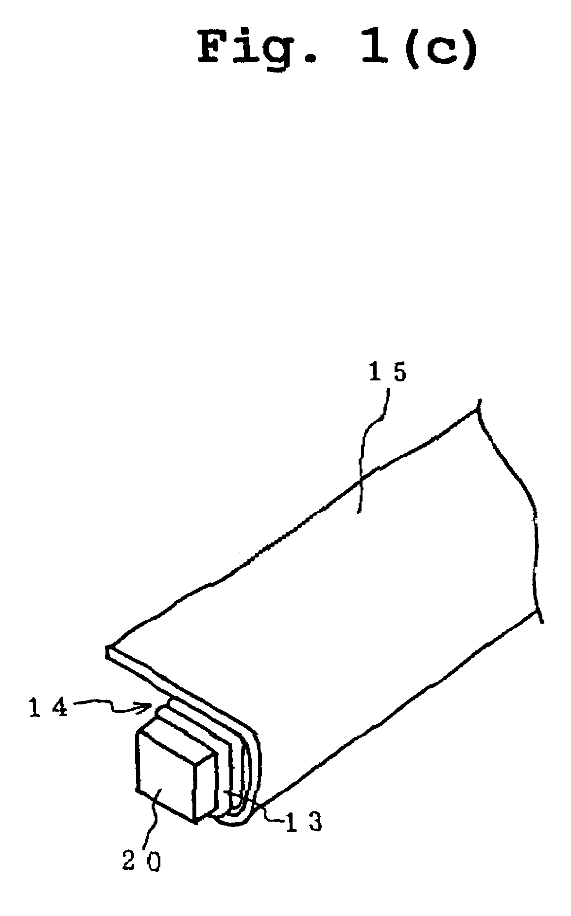
[0075]A polyester (manufactured by Toray Industries, Inc., Hytrel (trademark), softening temperature 204° C.) was applied to a Cu thin wire (diameter 18 μm) in a thickness of 4 μm, and the wire was wound to form a single roll layer around a core member (section: 180 mm×180 mm square prism) without forming a space between wires. A 100 μm thick fluorocarbon / acrylic film (manufactured by Denki Kagaku Kogyo K. K., DENKA DX-14™, softening temperature 150° C., elastic modulus 1.3 GPa) was layered on the single roll layer. This process was repeated to give a laminate alternately comprising 50 layers of a winding layer comprising Cu thin wires having a coating layer made from a polyester resin in one row and a fluorocarbon / acrylic film layer. The Cu thin wire of the winding layer was wound while changing the winding position between the odd-numbered winding layers and the even-numbered winding layers in the longitudinal direction of the core member in a closest packing state. This laminate ...

example 2

[0077]A polycarbodiimide resin (obtained by polymerizing 2,2-dimethyl-1,3-bis(4-aminophenoxy)propane (40 g), 3-methyl-1-phenyl-2-phospholene-1-oxide (1.14 g) and p-isopropylphenylisocyanate (2.19 g) in toluene at 80° C. for 2 hr, softening temperature 100° C.) was applied to a Cu thin wire (diameter 18 μm) in a thickness of 7.5 μm, and the wire was wound around the same core prism as used in Example 1 to form a single roll layer without forming a space between the wires. A 50 μm thick thermosetting epoxy film (softening temperature 100 ° C., elastic modulus 2 GPa) was applied on the single roll layer, which process was repeated to give a laminate alternately comprising 100 layers of a winding layer comprising Cu thin wires having a coating layer made from a polycarbodiimide resin in one row and an epoxy film layer. The thermosetting epoxy film used here was obtained by reacting a bisphenol A type epoxy resin with an acid anhydride hardener and a carboxyl group-containing liquid rubb...

example 3

[0079]An amideimide resin (softening temperature 170° C.) was applied to a Cu thin wire (diameter 18 μm) in a thickness of 3 μm, and the wire was wound around the same core member as used in Example 1 to form a single roll layer at a 48 μm interval. A 150 μm thick polycarbodiimide resin film (softening temperature 100° C.) was applied on the single roll layer, which process was repeated to give a laminate alternately comprising 100 layers of a winding layer comprising Cu thin wires having a coating layer made from an amideimide resin in one row and a polycarbodiimide resin film. All the Cu thin wire in the winding layers were wound such that the winding position of each Cu thin wire comes to the same position in the longitudinal direction of the core member. This laminate was made into a block under the conditions of 140° C., 1.96 MPa (polycarbodiimide resin alone softened and flew). The core member was removed and this block was sliced with a wire saw along the plane forming an ang...


PUM

PropertyMeasurementUnit
softening pointaaaaaaaaaa
outer diameteraaaaaaaaaa

Abstract

An anisotropic conductive film is prepared by winding an insulated wire around a core member to form one roll of a winding layer, placing an insulating resin film on the obtained winding layer, and repeating the step of winding the insulated wire and the step of placing the insulating resin film to give a laminate alternately having the winding layer comprising a single row of insulated wires and an insulating resin layer made from the insulating resin film. A coating layer and insulating resin layer are melted to integrate the winding layer and the insulating resin layer. The laminate then is sliced along a plane forming an angle with the insulated wire in a desired film thickness.

Description

CROSS-REFERENCE TO RELATED APPLICATION[0001]This patent application is a divisional of U.S. patent application Ser. No. 09 / 837,411, filed Apr. 18, 2001, now U.S. Pat. No. 6,566,608.TECHNICAL FIELD OF THE INVENTION[0002]The present invention relates to a production method of an anisotropic conductive film and an anisotropic conductive film produced by this method.BACKGROUND OF THE INVENTION[0003]Anisotropic conductive films have been widely used in the electronic industry as a connector for testing semiconductor devices and circuit boards, a connector of circuits between boards, a material for mounting a semiconductor device on a circuit board and the like. A known anisotropic conductive film is formed by dispersing conductive particles in a film made from an adhesive insulating resin. However, this anisotropic conductive film is subject to restriction because a fine pitch connection is difficult to achieve and a convex terminal (e.g., bump contact) is required as a connection termin...

Claims


Application Information

Patent Timeline
Patent Type & Authority Patents(United States)
IPC IPC(8): H01F7/127B21C23/08H01F5/02B29D7/00H01B5/16H01B13/00H01R11/01H01R13/24H01R43/00
CPCH01R43/007H01R13/2414Y10T29/49073Y10T29/49071Y10T29/4902Y10T29/49798Y10T29/5187
Inventor YAMAGUCHI, MIHOSUEHIRO, ICHIROASAI, FUMITERUHOTTA, YUJI
Owner NITTO DENKO CORP
Why Eureka
Try Eureka