Method of cleaning CVD equipment processing chamber

a technology of cvd equipment and processing chamber, which is applied in the direction of plasma technique, cleaning of hollow articles, coatings, etc., can solve the problems of dram or deposition failure, inability to clean, and increase the time required for cleaning, so as to achieve low cleaning operational cost and high efficiency

Active Publication Date: 2007-06-26
ASM JAPAN
View PDF7 Cites 351 Cited by
  • Summary
  • Abstract
  • Description
  • Claims
  • Application Information

AI Technical Summary

Benefits of technology

[0013]The second object of the present invention is to provide a remote pla

Problems solved by technology

When the deposits exfoliate, they cause particle contamination in a deposition process, resulting in wiring malfunction of devices such as DRAM or deposition failure.
In the case of the in-situ cleaning, however, because plasma is generated by applying high-frequency power to the upper electrode, which is used during a deposition process, ion collision is caused by charged particles generated in a space between the upper electrode and a susceptor which is the lower electrode.
As a result, sputtering of a surface of the upper electrode is caused, resulting in problems such as by-product generation and el

Method used


Image

  • Method of cleaning CVD equipment processing chamber
  • Method of cleaning CVD equipment processing chamber
  • Method of cleaning CVD equipment processing chamber

Examples


experiment 1

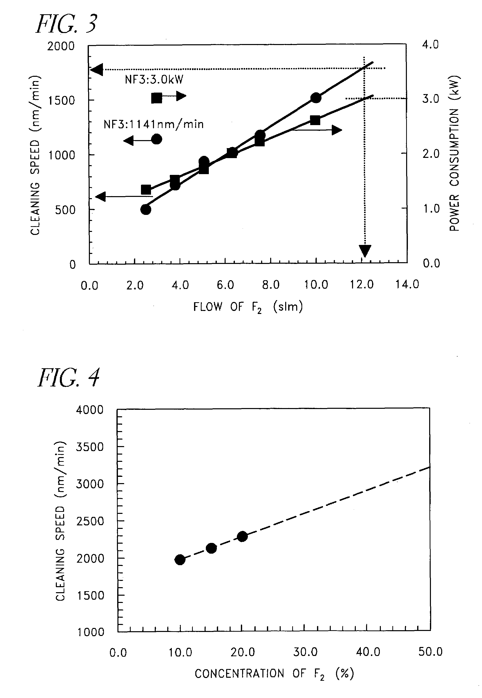
[0060]Comparative experiments of conventional remote plasma cleaning using a mixed gas of NF3 and Ar as cleaning gas and the remote plasma cleaning according to the present invention using a mixed gas of F2 and Ar as cleaning gas were conducted.

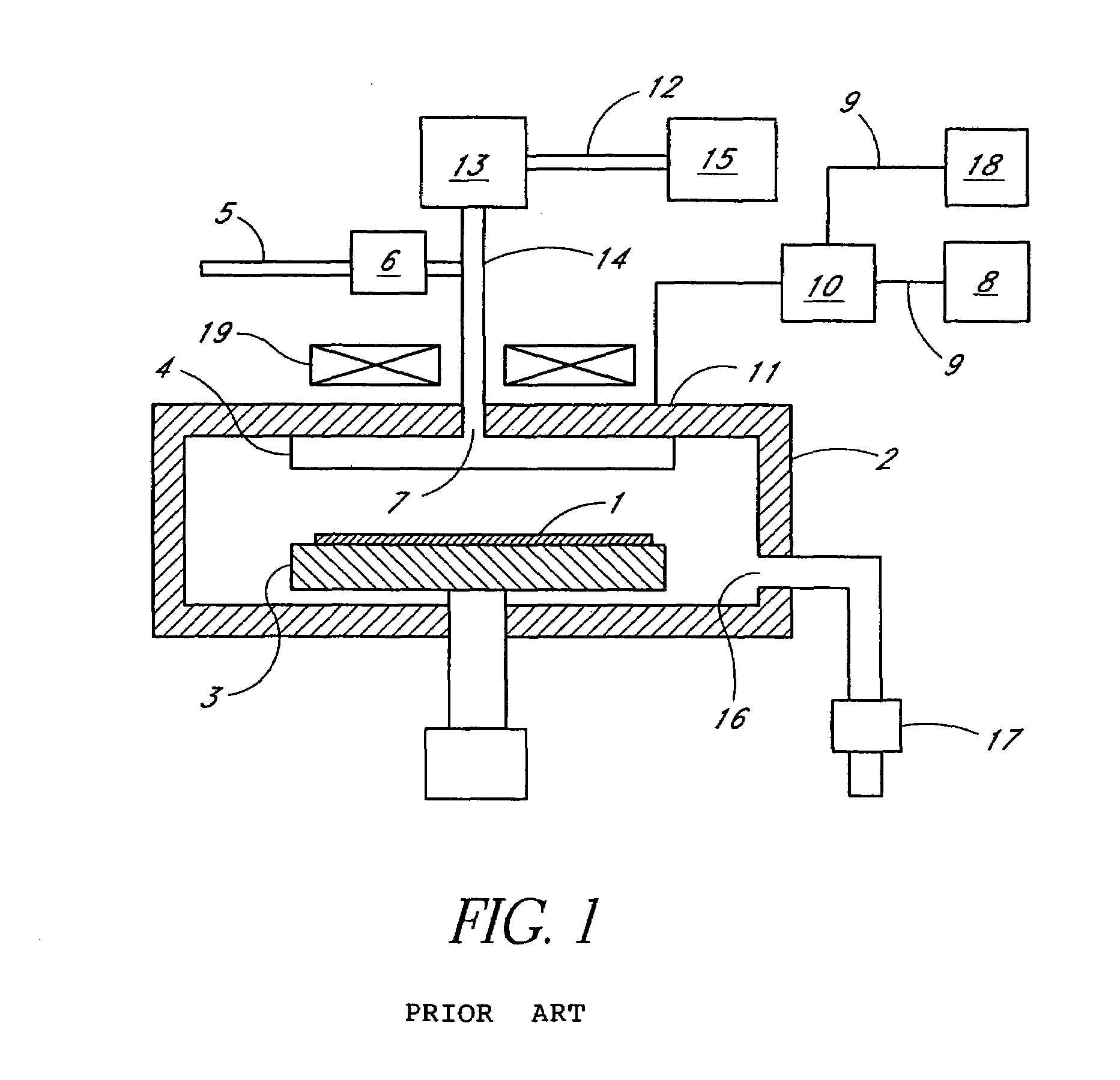
[0061]For the comparative experiments, a system with the same configuration as shown in FIG. 1 was used. With conditions of a TEOS flow of 115 sccm, an O2 flow of 1000 sccm, a reaction chamber pressure of 3.5 Torr, high-frequency power (13.56 MHz) at 315 w, high-frequency power (430 kHz) at 300 W, a gap distance of 10 mm, an upper electrode temperature of 130° C., a lower electrode temperature of 400° C., and a reaction chamber side-wall temperature of 120° C., a plasma oxide film was formed on a Ø200 mm silicon wafer. After deposition was completed, with conditions of an NF3 flow of 1.0 slm, an Ar flow of 2 slm, a reaction chamber pressure of 5 Torr, a gap distance of 14 mm, an upper electrode temperature of 130° C., a lower electrode temper...

experiment 2

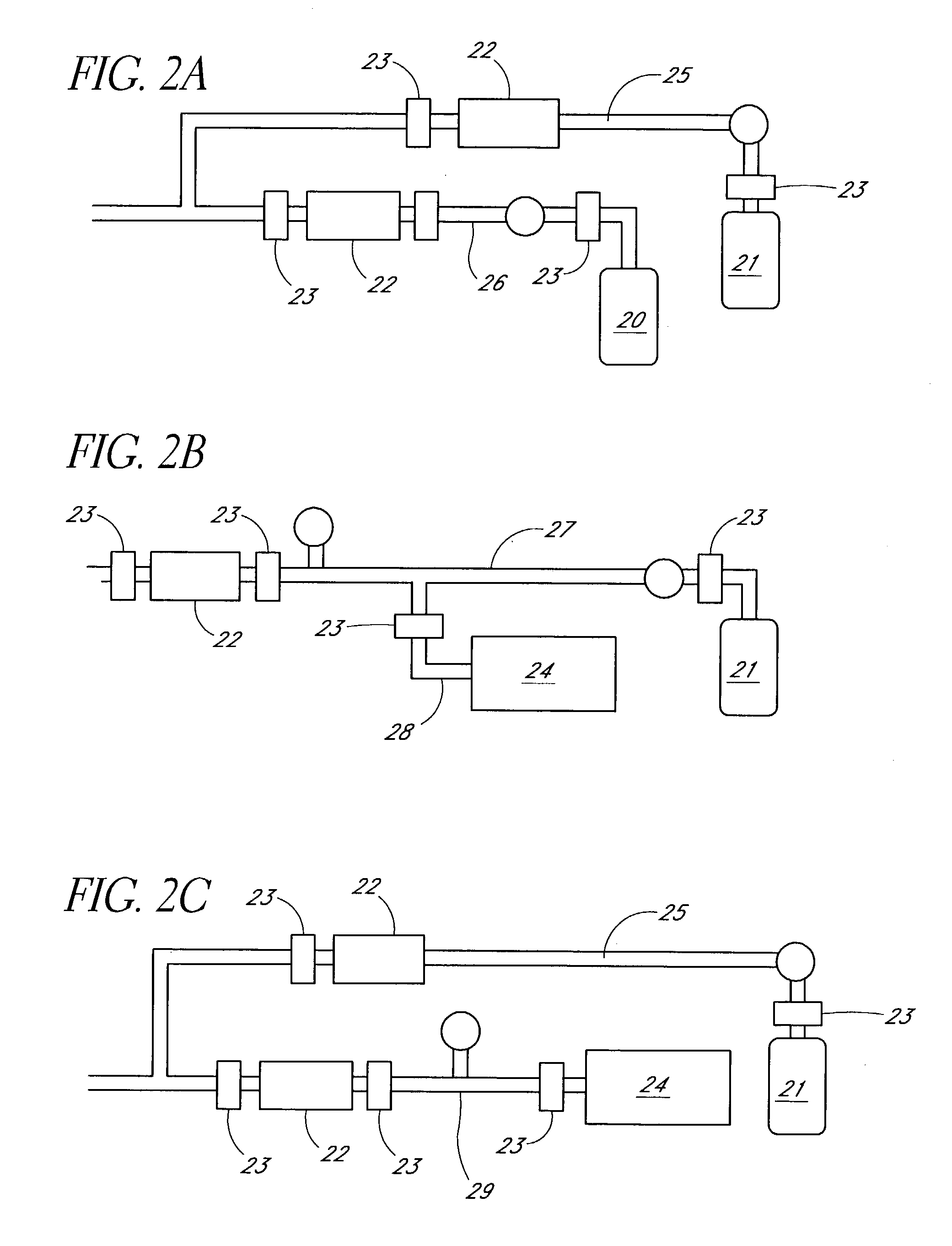
[0068]According to the remote plasma cleaning method according to the present invention, an evaluation experiment of the relation between pure-F2 concentration and cleaning rates was conducted. For this experiment, the preferred embodiment of the cleaning gas supplying means shown in FIG. 2a was used. In Experiment 2, by increasing only an Ar flow by releasing the valve 23 of the Ar gas cylinder 21, it was set up so that F2 concentration was able to be controlled at 20% or lower without altering a pure-F2 flow. Under the same deposition conditions as used in Experiment 1, a plasma oxide film of 1 μm was formed on a Ø200 mm silicon wafer. After deposition was completed, the silicon wafer was carried out from the reaction chamber. Cleaning was conducted. A flow of 20% F2 (80% diluted by Ar) was stabilized at 12 slm (a pure-F2 flow of 2.4 slm), which was the critical flow within power consumption of 3.0 kW in Experiment 1, and F2 concentration was 20% when an Ar flow was at 0 slm. An A...

experiment 3

[0073]To further improve cleaning efficiency of the reaction chamber, an evaluation experiment by device hardware was conducted. As a device, parallel-flat-plate plasma CVD equipment for 300 mm wafer processing manufactured by ASM Japan (Dragon™212) was used, and later replaced by Dragon™2300. As to the equipment concerned, as disclosed in Japanese Patent Application No. 2001-361669, which is incorporated herein by reference, a lower electrode is selected so that a value of a surface area of the lower electrode divided by a surface area of a wafer is in the range of 1.08 to 1.38, an upper electrode is selected so that a value of a surface area of the upper electrode divided by a surface area of the lower electrode is in the range of 1.05 to 1.44, and an upper electrode temperature is controlled in the range of 200° C. to 400° C.

[0074]When the equipment concerned and conventional plasma CVD equipment for 300 mm wafer processing shown in FIG. 1 are compared, in-plane film thickness ho...


PUM

PropertyMeasurementUnit
Temperatureaaaaaaaaaa
Fractionaaaaaaaaaa

Abstract

A method of remote plasma cleaning a processing chamber of CVD equipment, which has high cleaning rates, low cleaning operational cost and high efficiency, is provided. The method comprises supplying cleaning gas to the remote plasma-discharge device; activating the cleaning gas inside the remote plasma-discharge device; and bringing the activated cleaning gas into the processing chamber and which is characterized in that a mixed gas of F2 gas and an inert gas are used as the cleaning gas. A concentration of the F2 gas is 10% or higher. The F2 gas, which is a cleaning gas, is supplied to the remote plasma-discharge device from an F2 gas cylinder by diluting F2 gas at a given concentration by an inert gas.

Description

BACKGROUND OF THE INVENTION[0001]1. Field of the Invention[0002]The present invention relates to a method of cleaning inside the processing chamber of CVD equipment used for semiconductor manufacturing. The invention particularly relates to a method of cleaning inside the processing chamber employing a remote plasma.[0003]2. Description of the Related Art[0004]In CVD (Chemical Vapor Deposition) equipment used for semiconductor manufacturing or deposition equipment including sputtering equipment, if deposition onto an object to be processed (e.g., a semiconductor wafer) is performed continuously, deposits adhere to internal walls of a processing chamber, etc. other than the object to be processed. When the deposits exfoliate, they cause particle contamination in a deposition process, resulting in wiring malfunction of devices such as DRAM or deposition failure. Consequently, it is required to clean inside a processing chamber with a given cycle.[0005]Up to now, as disclosed in Japane...

Claims


Application Information

Patent Timeline
IPC IPC(8): B08B9/093B08B7/00C23C16/44H01L21/3065H01L21/31
CPCB08B7/0035C23C16/4405H01J37/32862Y10S134/902Y10S438/905
Inventor ARAI, HIROFUMIFUKUDA, HIDEAKI
Owner ASM JAPAN
Why Eureka
Try Eureka