Filter circuit

a filter circuit and circuit technology, applied in the field of gmc (transconductancec) filter circuits, can solve the problem of increasing power consumption

Inactive Publication Date: 2007-07-03
SONY CORP
View PDF5 Cites 17 Cited by
  • Summary
  • Abstract
  • Description
  • Claims
  • Application Information

AI Technical Summary

Benefits of technology

[0021]It is therefore desirable to provide a filter circuit able to make the filter frequency characteristic variable up to over one hundredfold with a fine resolution of about 1% of the signal bandwidth and having steps of variation of frequency proportional to the filter frequency characteristic by a simple method without a great increase of the overall circuit scale.

Problems solved by technology

On the other hand, there are the defects that a prepositioned filter is required for preventing aliasing due to the sampling operation and that a broadband operational amplifier is necessary in order to realize circuit settling in a clock cycle, so, particularly in a high frequency filter, the power consumption tends to increase.

Method used


Image

  • Filter circuit
  • Filter circuit
  • Filter circuit

Examples


first embodiment

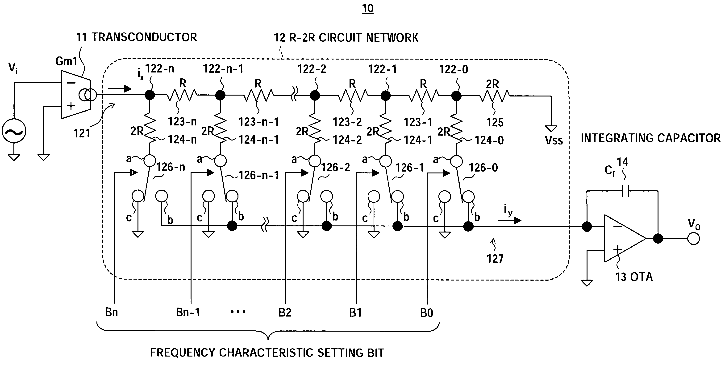
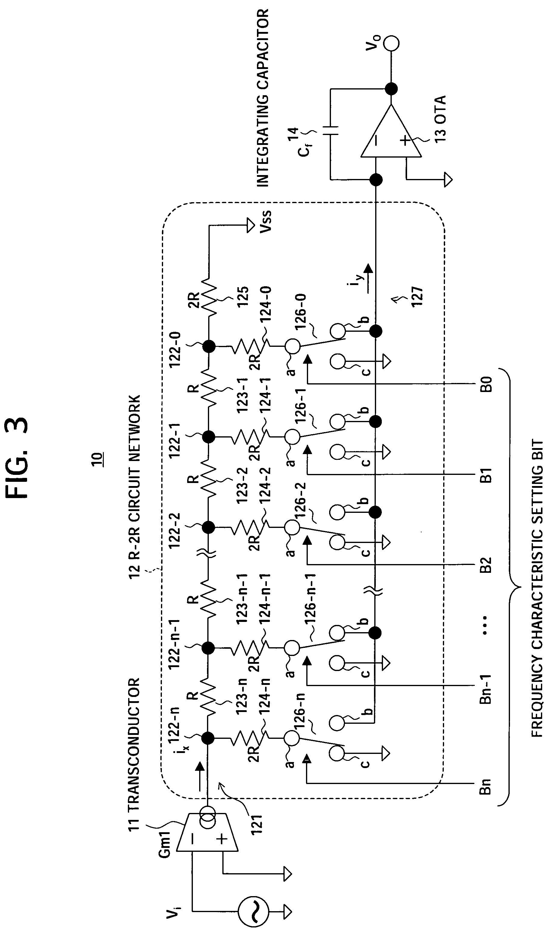
[0048]FIG. 3 is a circuit diagram of a filter circuit according to a first embodiment of the present invention.

[0049]The filter circuit 10 has, as shown in FIG. 3, a transconductor (Gm1) 11 outputting a current ix proportional to an input voltage Vi, an R-2R resistor circuit network 12 able to change the frequency characteristic of the output current of the transconductor with a precision of a bit width of (n+1) in accordance with (n+1) bit frequency characteristic setting bit data, an operational transconductance amplifier (hereinafter referred to as an “OTA”) 13 having an input terminal connected to the current output line of the R-2R resistor circuit network 12, and an integrating capacitor (Cf) 14 connected between the input terminal (−) and the output terminal of the OTA 13. Note that n is an integer of 1 or more.

[0050]The R-2R resistor circuit network 12 includes, as shown in FIG. 3, (n+1) number of branch nodes 122-n to 122-0 formed on a current propagation line 121 for propa...

second embodiment

[0098]FIG. 5 is a circuit diagram of a filter circuit according to a second embodiment of the present invention.

[0099]The difference of the filter circuit 10A according to the second embodiment from the filter circuit 10 according to the first embodiment resides in that the input terminal of the current follower 15 is connected in place of connecting the OTA to the current output line of the R-2R resistor circuit network 12 and that the integrating capacitor 14 is connected between the output terminal of the current follower (CF) 15 and the low impedance analog midpoint (ground potential).

[0100]In the second embodiment, in the R-2R resistor circuit network 12, there is a path through which each branch current flows to the next current follower 15 and a path through which it flows to a low impedance analog midpoint (ground potential). The path can be selected by the digital control bits Bn to B0 for each branch current. Here, the set bit width n+1 may be any width. The setting method...

third embodiment

[0108]FIG. 7 is a circuit diagram of a filter circuit according to a third embodiment of the present invention.

[0109]The third embodiment combines the first embodiment and the second embodiment.

[0110]Namely, it is also possible to realize the integrating capacitor portion of the second embodiment by the OTA-C as in the first embodiment (Gm-R2R-CF-OTA-C filter). Specifically, the input terminal of the OTA 13 is connected to the output terminal of the current follower 15, and the integrating capacitor 14 is connected between the input terminal and output terminal of the OTA 13.

[0111]The advantage of the third embodiment resides in that the input impedance may be sufficiently lowered by the current follower (CF) 15 and in addition the DC gain of the integrator may be set extremely large by the OTA 13, that is, it is possible to set the first pole frequency low. By this, even when the number of stages of R-2R is increased and the frequency characteristic is set low, a good integrating c...


PUM

PropertyMeasurementUnit
cutoff frequencyaaaaaaaaaa

Abstract

An R-2R resistor circuit network 12 used in a filter circuit according to the present invention has a path through which each branch current flows to a next integrating capacitor and a path through which each branch current flows to a low impedance analog midpoint (ground potential) Vss. The path can be selected by digital control bit data Bn to B0 for each branch current. By this, a frequency characteristic of a filter using an integrator as a component may be changed with an accuracy of (½n+1)(Gm1) / Cf from (½n+1)(Gm1) / Cf to ((2n+1−½n+1)(Gm1)Cf. As a result, by setting the setting bit width to 7 (n=6), a variable range of the frequency characteristic of over one hundredfold may be easily realized.

Description

CROSS REFERENCES TO RELATED APPLICATIONS[0001]The present invention contains subject matter related to Japanese Patent Application No. 2004-111427 filed in the Japan Patent Office on Apr. 5, 2004, the entire contents of which being incorporated herein by reference.BACKGROUND OF THE INVENTION[0002]1. Field of the Invention[0003]The present invention relates to a filter circuit such as a continuous time analog integrated filter circuit, more particularly relates to a Gm-C (Transconductance-C) filter circuit having an integrator as a component, and to a method for realizing a system able to change the cutoff frequency, pole, or zero filter frequency characteristic up to over one hundredfold with a fine resolution of about 1% of a signal bandwidth.[0004]2. Description of the Related Art[0005]In the past, as analog integrated filters mainly using active elements, discrete time filters such as switched capacitor filters (SCFs) and continuous time filters such as transconductance-capacitor...

Claims


Application Information

Patent Timeline
Patent Type & Authority Patents(United States)
IPC IPC(8): H03K5/00H03H11/04G11B5/09H03H11/12
CPCH03H11/1291A47G21/103
Inventor HASEGAWA, YASUMASA
Owner SONY CORP
Why Eureka
Try Eureka