Surface finishing of SOI substrates using an EPI process

a technology of surface finishing and soi substrate, applied in the field of manufacture of objects, can solve the problems of limiting the degree of integration achievable in a given chip, conventional isolation techniques consume a considerable amount of valuable wafer surface area on the chip, and the technique is not free from limitations, so as to improve the degree of integration, reduce the predetermined surface roughness value, and improve the crystal structure

Inactive Publication Date: 2007-08-07
SILICON GENERAL CORPORATION
View PDF50 Cites 6 Cited by
  • Summary
  • Abstract
  • Description
  • Claims
  • Application Information

AI Technical Summary

Benefits of technology

[0009]In an alternative embodiment, the present invention provides a method for treating a film of material, which can be defined on a substrate, e.g., silicon. The method includes providing a substrate comprising a cleaved surface, which is characterized by a predetermined surface roughness value. The substrate also has a distribution of hydrogen bearing particles defined from the cleaved surface to a region underlying the cleaved surface. The method also includes increasing a temperature of the cleaved surface to greater than about 1,000 Degrees Celsius while maintaining the cleaved surface in a hydrogen etchant bearing environment to reduce the predetermined surface roughness value by about fifty percent and greater. Other embodiments include a temperature range from about 900 to about 1,000 Degrees Celsius and greater for silicon. Preferably, the value can be reduced by about eighty or ninety percent and greater, depending upon the embodiment.
[0010]Numerous benefits are achieved by way of the present invention over pre-existing techniques. For example, the present invention provides an efficient technique for forming a substantially uniform surface on an SOI wafer. Additionally, the substantially uniform surface is made by way of common hydrogen treatment and etching techniques, which can be found in conventional epitaxial tools. Furthermore, the present invention provides a novel uniform layer, which can be ready for the manufacture of integrated circuits. The present invention also relies upon standard fabrication gases such as HCl and hydrogen gas. In preferred embodiments, the present invention can improve bond interface integrity, improve crystal structure, and reduce defects in the substrate simultaneously during the process. Depending upon the embodiment, one or more of these benefits is present. These and other advantages or benefits are described throughout the present specification and are described more particularly below.

Problems solved by technology

These techniques, however, are not free from limitations.
For example, conventional isolation techniques consume a considerable amount of valuable wafer surface area on the chip, and often generate a non-planar surface as an artifact of the isolation process.
Either or both of these considerations generally limit the degree of integration achievable in a given chip.
Additionally, trench isolation often requires a process of reactive ion etching, which is extremely time consuming and can be difficult to achieve accurately.
Many problems, however, that have already been solved regarding fabricating devices on bulk silicon wafers remain to be solved for fabricating devices on SOI wafers.
CMP is generally time consuming and expensive, and can be difficult to perform cost efficiently to remove surface non-uniformities.
That is, a CMP machine is expensive and requires large quantities of slurry mixture, which is also expensive.

Method used


Image

  • Surface finishing of SOI substrates using an EPI process
  • Surface finishing of SOI substrates using an EPI process
  • Surface finishing of SOI substrates using an EPI process

Examples


Embodiment Construction

[0014]According to the present invention, a technique for treating a film of material is provided. More particularly, the present invention provides a method for treating a cleaved surface and / or an implanted surface using a combination of thermal treatment and chemical reaction, which can form a substantially smooth film layer from the cleaved surface. The invention will be better understood by reference to the Figs. and the descriptions below.

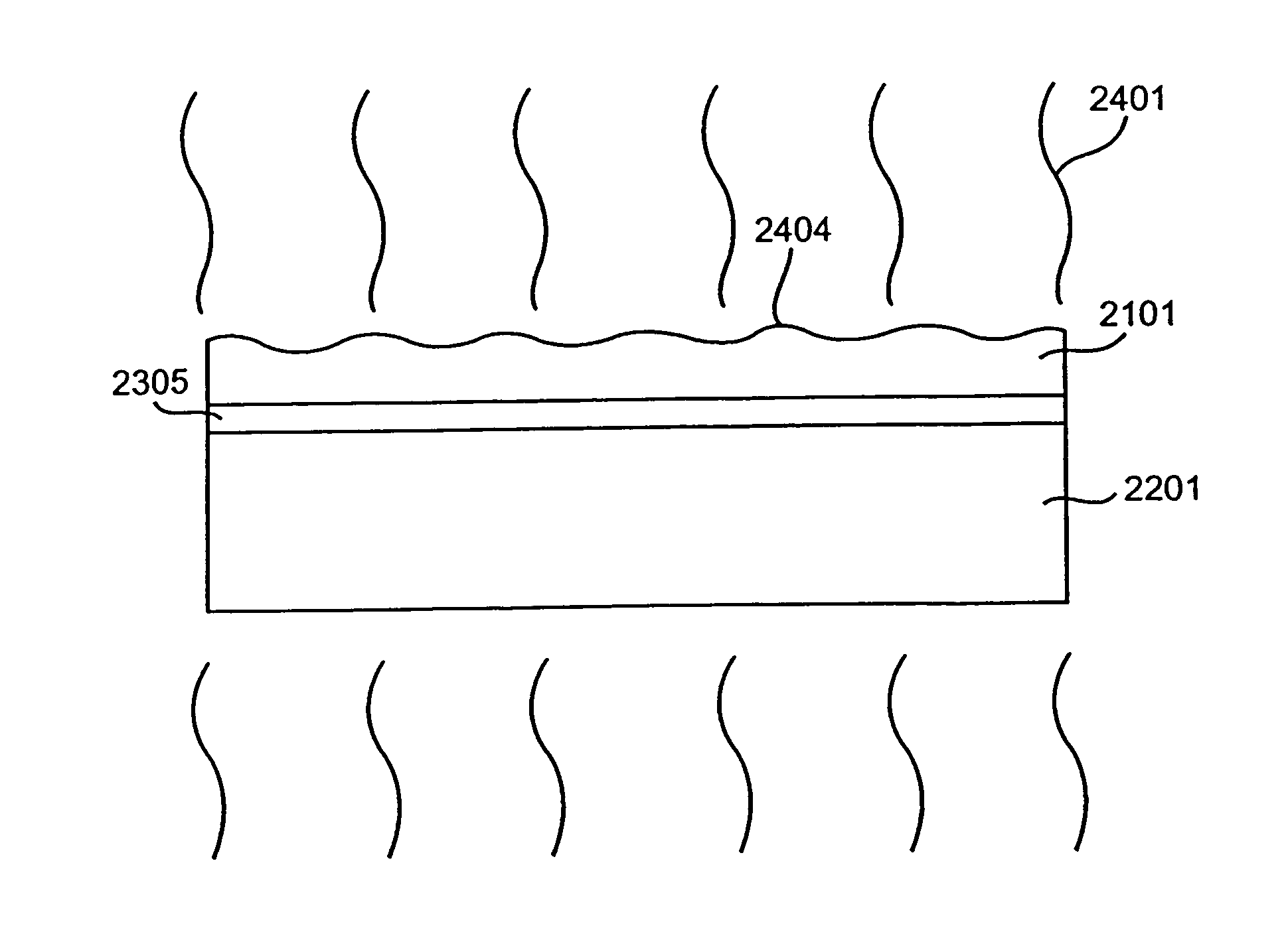
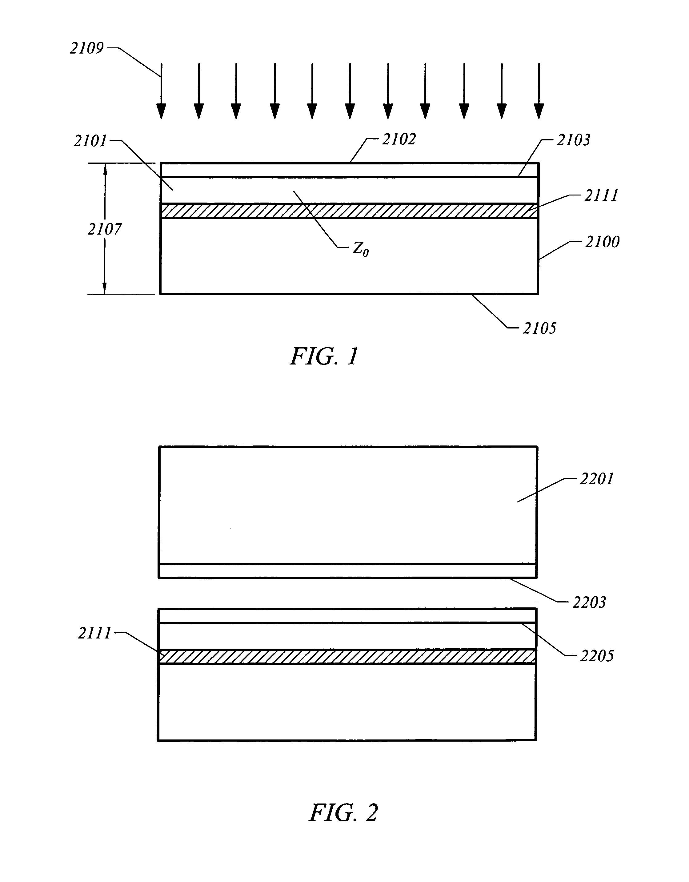
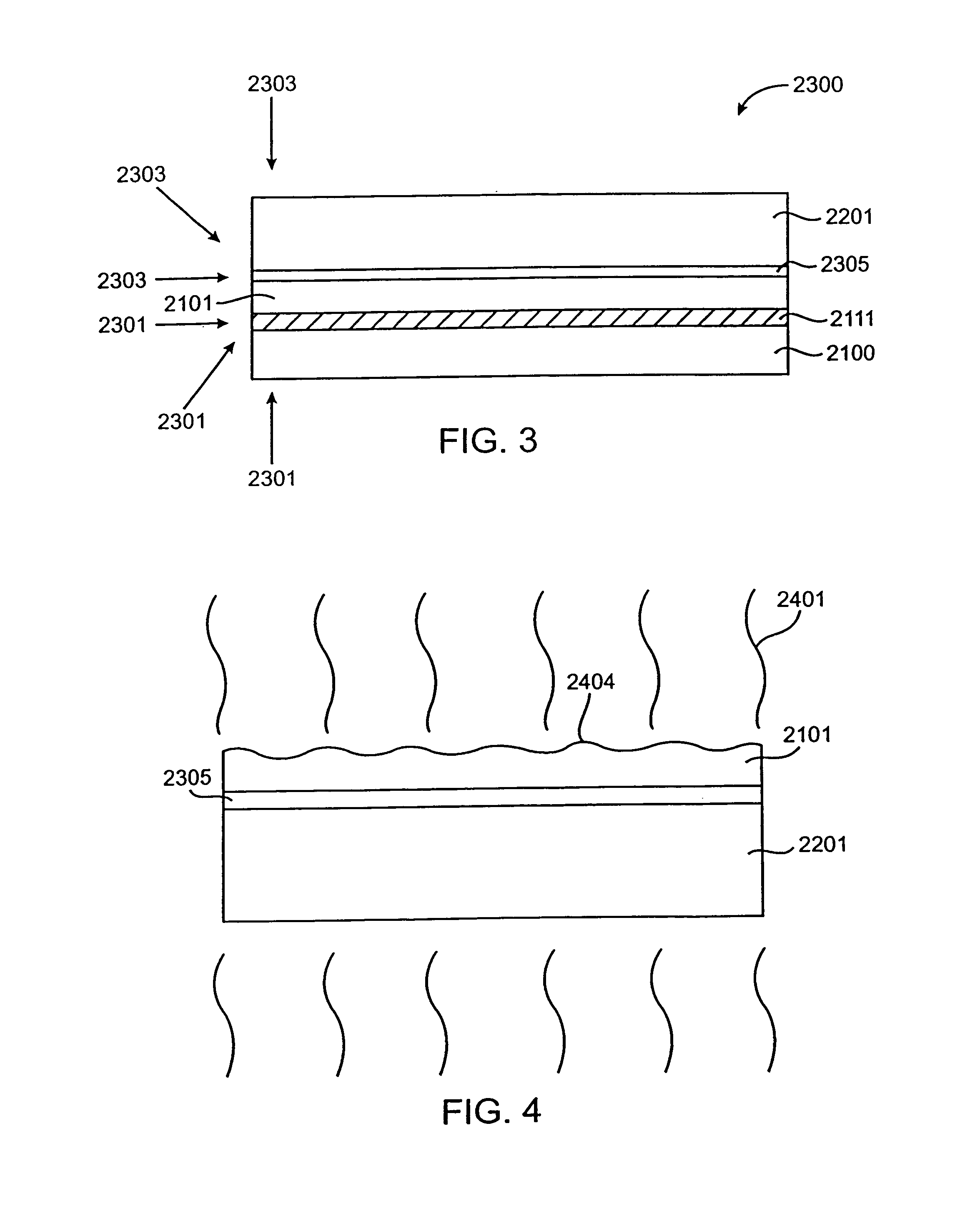
[0015]A process for fabricating a silicon-on-insulator substrate according to the present invention may be briefly outlined as follows:[0016](1) Provide a donor silicon wafer (which may be coated with a dielectric material);[0017](2) Introduce particles into the silicon wafer to a selected depth to define a thickness of silicon film;[0018](3) Provide a target substrate material (which may be coated with a dielectric material);[0019](4) Bond the donor silicon wafer to the target substrate material by joining the implanted face to the target su...


PUM

PropertyMeasurementUnit
pressureaaaaaaaaaa
surface roughnessaaaaaaaaaa

Abstract

A method for treating a film of material, which can be defined on a substrate, e.g., silicon. The method includes providing a substrate comprising a cleaved surface, which is characterized by a predetermined surface roughness value. The substrate also has a distribution of hydrogen bearing particles defined from the cleaved surface to a region underlying said cleaved surface. The method also includes increasing a temperature of the cleaved surface to greater than about 1,000 Degrees Celsius while maintaining the cleaved surface in an etchant bearing environment to reduce the predetermined surface roughness value by about fifty percent and greater. Preferably, the value can be reduced by about eighty or ninety percent and greater, depending upon the embodiment.

Description

[0001]This is a continuation of U.S. patent application Ser. No. 09 / 399,985, filed on Sep. 20, 1999, now U.S. Pat. No. 6,287,941, which claims priority to U.S. Provisional Patent Application No. 60 / 130,423, filed on Apr. 21, 1999, now abandoned which are incorporated by reference herein for all purposes.BACKGROUND OF THE INVENTION[0002]The present invention relates to the manufacture of objects. More particularly, the present invention provides a technique for improving surface texture or surface characteristics of a film of material, e.g., silicon, silicon germanium, or others. The present invention can be applied to treating or smoothing a cleaved film from a layer transfer process for the manufacture of integrated circuits, for example. But it will be recognized that the invention has a wider range of applicability; it can also be applied to smoothing a film for other substrates such as multi-layered integrated circuit devices, three-dimensional packaging of integrated semiconduc...

Claims


Application Information

Patent Timeline
Patent Type & Authority Patents(United States)
IPC IPC(8): H01L21/30H01L21/302H01L21/02H01L21/20H01L21/324H01L21/762H01L27/12
CPCH01L21/2007H01L21/3065H01L21/76254Y10S438/967H01L21/84
Inventor KANG, SIEN G.MALIK, IGOR J.
Owner SILICON GENERAL CORPORATION
Why Eureka
Try Eureka